 搜索
搜索
 发布采购
发布采购
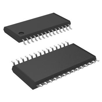
- 封装:28-TSSOP(0.173",4.40mm 宽)
- RoHS:无铅 / 符合限制有害物质指令(RoHS)规范要求
- 包装方式:管件
- 参考价格:$10.688-$9.7376
更新日期:2024-04-01 00:04:00
产品简介:MuxIt ? pll 倍频器
查看详情- 封装:28-TSSOP(0.173",4.40mm 宽)
- RoHS:无铅 / 符合限制有害物质指令(RoHS)规范要求
- 包装方式:管件
- 参考价格:$10.688-$9.7376
SN65LVDS150PW 供应商
- 公司
- 型号
- 品牌
- 封装/批号
- 数量
- 地区
- 日期
- 说明
- 询价
-
TI
-
原厂原装
22+ -
3288
-
上海市
-
-
-
一级代理原装
-
TI
-
-
2019+ -
5800
-
上海市
-
-
-
全新原装现货
-
TI(德州仪器)
-
TSSOP-28
2022+ -
12000
-
上海市
-
-
-
原装可开发票
-
TI/BB
-
28TSSOP
23+ -
15000
-
上海市
-
-
-
中国区代理原装进口特价
-
TI
-
-
21+ -
2000
-
上海市
-
-
-
原装现货,品质为先!请来电垂询!
-
-
23+ -
5800
-
上海市
-
-
-
进口原装现货,杜绝假货。
SN65LVDS150PW 中文资料属性参数
- 标准包装:50
- 类别:集成电路 (IC)
- 家庭:时钟/计时 - 时钟发生器,PLL,频率合成器
- 系列:MuxIt™
- 类型:PLL 倍频器
- PLL:是
- 输入:LVDS
- 输出:LVDS,LVTTL
- 电路数:1
- 比率 - 输入:输出:1:2
- 差分 - 输入:输出:是/是
- 频率 - 最大:400MHz
- 除法器/乘法器:是/是
- 电源电压:3 V ~ 3.6 V
- 工作温度:-40°C ~ 85°C
- 安装类型:表面贴装
- 封装/外壳:28-TSSOP(0.173",4.40mm 宽)
- 供应商设备封装:28-TSSOP
- 包装:管件
- 配用:296-9620-ND - EVAL MOD SN65LVDS150/151/152
- 其它名称:296-9737-5
产品特性
- A Member of the MuxItTM Serializer- Deserializer Building-Block Chip Family
- Pin Selectable Frequency Multiplier Ratios Between 4 and 40
- Input Clock Frequencies From 5 to 50 MHz
- Multiplied Clock Frequencies up to 400MHz
- Internal Loop Filters and Low PLL-Jitter of 20 ps RMS Typical at 200 MHz
- LVDS Compatible Differential Inputs and Outputs Meet or Exceed the Requirements of ANSI EIA/TIA-644-A
- LVTTL Compatible Inputs Are 5 V Tolerant
- LVDS Inputs and Outputs ESD Protection Exceeds 12 kV HBM
- Operates From a Single 3.3 V Supply
- Packaged in 28-Pin Thin Shrink Small-Outline Package With 26 mil Terminal Pitch
产品概述
The MuxIt is a family of general-purpose, multiple-chip building blocks for implementing parallel data serializers and deserializers. The system allows for wide parallel data to be transmitted through a reduced number of differential transmission lines over distances greater than can be achieved with a single-ended (e.g., LVTTL or LVCMOS) data interface. The number of bits multiplexed per transmission line is user selectable, allowing for higher transmission efficiencies than with other existing fixed ratio solutions. Muxlt utilizes the LVDS (TIA/EIA-644) low voltage differential signaling technology for communications between the data source and data destination.
The MuxIt family initially includes three devices supporting simplex communications;
The SN65LVDS150 Phase Locked Loop-Frequency Multiplier, The SN65LVDS151 Serializer-Transmitter, and The SN65LVDS152 Receiver-Deserializer.
The SN65LVDS150 is a PLL based frequency multiplier designed for use with the other members of the MuxIt family of serializers and deserializers. The frequency multiplication ratio is pin selectable over a wide range of values from 4 through 40 to accommodate a broad spectrum of user needs. No external filter components are needed. A PLL lock indicator output is available which may be used to enable link data transfers.
The design of the SN65LVDS150 allows it to be used at either the transmit end or the receive end of the MuxIt serial link. The differential clock reference input (CRI) is driven by the system's parallel data clock when at the source end of the link, or by the link clock when at the destination end of the link. The differential clock reference input may be driven by either an LVDS differential signal, or by a single ended clock of either polarity. For single-ended use the nonclocked input is biased to the logic threshold voltage. A VCC/2 threshold reference, VT, is provided on a pin adjacent the differential CRI pins for convenience when the input is used in a single-ended mode.
The multiplied clock output (MCO) is an LVDS differential signal used to drive the high-speed shift registers in either the SN65LVDS151 serializer-transmitter or the SN65LVDS152 receiver-deserializer. The link clock reference output (LCRO) is an LVDS differential signal provided to the SN65LVDS151 serializer-transmitter for transmission over the link.
An internal power on reset and an enable input (EN) control the operation of the SN65LVDS150. When VCC is below 1.5 V, or when EN is low, the device is in a low power disabled state and the MCO and LCRO differential outputs are in a high-impedance state. When VCC is above 3 V and EN is high, the device and the two differential outputs are enabled and operating to specifications. The link clock reference output enable input (LCRO_EN) is used to turn off the LCRO output when it is not being used. A band select input (BSEL) is used to optimize the VCO performance as a function of M-clock frequencies and M multiplier that is being used: The fmax parameter in the switching characteristic table includes details on the MCO frequency and choices of BSEL and M.
SN65LVDS150PW 数据手册
| 数据手册 | 说明 | 数量 | 操作 |
|---|---|---|---|
 SN65LVDS150PW SN65LVDS150PW
|
IC MUXIT PLL FREQ MULT 28-TSSOP |
18页,374K | 查看 |
SN65LVDS150PW 相关产品
- 74HCT4046AD,118
- AD809BRZ-REEL7
- AD9512BCPZ-REEL7
- AD9513BCPZ
- AD9513BCPZ-REEL7
- AD9516-2BCPZ
- AD9516-3BCPZ-REEL7
- AD9517-0ABCPZ-RL7
- AD9517-1ABCPZ
- AD9517-1ABCPZ-RL7
- AD9517-2ABCPZ-RL7
- AD9517-3ABCPZ
- AD9517-3ABCPZ-RL7
- AD9517-4ABCPZ
- AD9517-4ABCPZ-RL7
- AD9518-0ABCPZ
- AD9518-0ABCPZ-RL7
- AD9518-1ABCPZ
- AD9518-1ABCPZ-RL7
- AD9518-2ABCPZ
- AD9518-2ABCPZ-RL7
- AD9518-3ABCPZ-RL7
- AD9518-4ABCPZ
- AD9518-4ABCPZ-RL7
- AD9520-0BCPZ
- AD9522-1BCPZ
- AD9522-2BCPZ
- AD9522-4BCPZ
- AD9522-4BCPZ-REEL7
- AD9522-5BCPZ