 搜索
搜索
 发布采购
发布采购
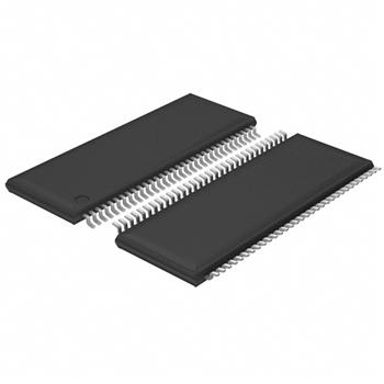
- 封装:64-TFSOP (0.240",6.10mm 宽)
- RoHS:无铅 / 符合限制有害物质指令(RoHS)规范要求
- 包装方式:管件
- 参考价格:$9.3072
更新日期:2024-04-01 00:04:00
产品简介:双路 8 端口 LVDS 中继器
查看详情- 封装:64-TFSOP (0.240",6.10mm 宽)
- RoHS:无铅 / 符合限制有害物质指令(RoHS)规范要求
- 包装方式:管件
- 参考价格:$9.3072
SN65LVDS117DGGG4 供应商
- 公司
- 型号
- 品牌
- 封装/批号
- 数量
- 地区
- 日期
- 说明
- 询价
-
TI
-
原厂原装
22+ -
3288
-
上海市
-
-
-
一级代理原装
SN65LVDS117DGGG4 中文资料属性参数
- 标准包装:25
- 类别:集成电路 (IC)
- 家庭:接口 - 信号缓冲器,中继器,分配器
- 系列:65LVDS
- 类型:转发器
- Tx/Rx类型:LVDS
- 延迟时间:4.5ns
- 电容 - 输入:5pF
- 电源电压:3 V ~ 3.6 V
- 电流 - 电源:122mA
- 安装类型:表面贴装
- 封装/外壳:64-TFSOP (0.240",6.10mm 宽)
- 供应商设备封装:64-TSSOP
- 包装:管件
产品特性
- Two Line Receivers and Eight ('109) or Sixteen ('117) Line Drivers Meet or Exceed the Requirements of ANSI EIA/TIA-644 Standard
- Typical Data Signaling Rates to 400 Mbps or Clock Frequencies to 400 MHz
- Outputs Arranged in Pairs From Each Bank
- Enabling Logic Allows Individual Control of Each Driver Output Pair, Plus All Outputs
- Low-Voltage Differential Signaling With Typical Output Voltage of 350 mV and a 100-Ω Load
- Electrically Compatible With LVDS, PECL, LVPECL, LVTTL, LVCMOS, GTL, BTL, CTT, SSTL, or HSTL Outputs With External Termination Networks
- Propagation Delay Times < 4.5 ns
- Output Skew Less Than 550 ps Bank Skew Less Than150 ps Part-to-Part Skew Less Than 1.5 ns
- Total Power Dissipation Typically <500 mW With All Ports Enabled and at 200 MHz
- Driver Outputs or Receiver Input Equals High Impedance When Disabled or With VCC < 1.5 V
- Bus-Pin ESD Protection Exceeds 12 kV
- Packaged in Thin Shrink Small-Outline Package With 20-Mil Terminal Pitch
产品概述
The SN65LVDS109 and SN65LVDS117 are configured as two identical banks, each bank having one differential line receiver connected to either four ('109) or eight ('117) differential line drivers. The outputs are arranged in pairs having one output from each of the two banks. Individual output enables are provided for each pair of outputs and an additional enable is provided for all outputs.The line receivers and line drivers implement the electrical characteristics of low-voltage differential signaling (LVDS). LVDS, as specified in EIA/TIA-644, is a data signaling technique that offers low power, low noise emission, high noise immunity, and high switching speeds. (Note: The ultimate rate and distance of data transfer is dependent upon the attenuation characteristics of the media, the noise coupling to the environment, and other system characteristics.)The intended application of these devices, and the LVDS signaling technique, is for point-to-point or point-to-multipoint (distributed simplex) baseband data transmission on controlled impedance media of approximately 100 Ω. The transmission media may be printed-circuit board traces, backplanes, or cables. The large number of drivers integrated into the same silicon substrate, along with the low pulse skew of balanced signaling, provides extremely precise timing alignment of the signals being repeated from the inputs. This is particularly advantageous for implementing system clock and data distribution trees.The SN65LVDS109 and SN65LVDS117 are characterized for operation from –40°C to 85°C.
SN65LVDS117DGGG4 数据手册
| 数据手册 | 说明 | 数量 | 操作 |
|---|---|---|---|
 SN65LVDS117DGGG4 SN65LVDS117DGGG4
|
Dual 8-Port LVDS Repeater 64-TSSOP -40 to 85 |
24页,503K | 查看 |
SN65LVDS117DGGG4 相关产品
- DS2175S
- DS2176Q
- ISL33001IRT2Z
- ISL33001IRTZ
- ISL33001IUZ-T
- ISL33002IRT2Z
- ISL33002IRTZ
- ISL33003IRT2Z
- ISL33003IRTZ
- ISL33003IUZ-T
- LTC4312CDE#PBF
- LTC4312IDE#PBF
- LTC4312IMS#PBF
- LTC4312IMS#TRPBF
- LTC4313CDD-1#PBF
- LTC4313CMS8-1#PBF
- LTC4313CMS8-2#PBF
- LTC4313CMS8-3#PBF
- LTC4313IMS8-1#PBF
- LTC4313IMS8-2#PBF
- LTC4313IMS8-3#PBF
- LTC4314CGN#PBF
- LTC4314CUDC#PBF
- LTC4314IGN#PBF
- LTC4314IUDC#PBF
- LTC4315CDE#PBF
- LTC4315CMS#PBF
- LTC4315IDE#PBF
- LTC4315IMS#PBF
- MAX9150EUI+