 搜索
搜索
 发布采购
发布采购
- 封装:16-TSSOP(0.173",4.40mm 宽)
- RoHS:无铅 / 符合限制有害物质指令(RoHS)规范要求
- 包装方式:带卷 (TR)
- 参考价格:$2.062
更新日期:2024-04-01 00:04:00

产品简介:1 LVTTL:4 LVDS 时钟扇出缓冲器
查看详情- 封装:16-TSSOP(0.173",4.40mm 宽)
- RoHS:无铅 / 符合限制有害物质指令(RoHS)规范要求
- 包装方式:带卷 (TR)
- 参考价格:$2.062
SN65LVDS105PWR 供应商
- 公司
- 型号
- 品牌
- 封装/批号
- 数量
- 地区
- 日期
- 说明
- 询价
-
TI
-
原厂原装
22+ -
3288
-
上海市
-
-
-
一级代理原装
-
TI/德州仪器
-
TSSOP16
21+ -
10000
-
杭州
-
-
-
只做原装现货,大量现货热卖
SN65LVDS105PWR 中文资料属性参数
- 标准包装:2,000
- 类别:集成电路 (IC)
- 家庭:接口 - 驱动器,接收器,收发器
- 系列:65LVDS
- 类型:时钟缓冲器
- 驱动器/接收器数:4/1
- 规程:LVDS
- 电源电压:3 V ~ 3.6 V
- 安装类型:表面贴装
- 封装/外壳:16-TSSOP(0.173",4.40mm 宽)
- 供应商设备封装:16-TSSOP
- 包装:带卷 (TR)
产品特性
- Receiver and Drivers Meet or Exceed the Requirements of ANSI EIA/TIA-644 Standard SN65LVDS105 Receives Low-Voltage TTL (LVTTL) Levels SN65LVDS104 Receives Differential Input Levels, ±100 mV
- SN65LVDS105 Receives Low-Voltage TTL (LVTTL) Levels
- SN65LVDS104 Receives Differential Input Levels, ±100 mV
- Typical Data Signaling Rates to 400 Mbps or Clock Frequencies to 400 MHz
- Operates From a Single 3.3-V Supply
- Low-Voltage Differential Signaling With Typical Output Voltage of 350 mV and a 100-Ω Load
- Propagation Delay Time SN65LVDS105 – 2.2 ns (Typ) SN65LVDS104 – 3.1 ns (Typ)
- SN65LVDS105 – 2.2 ns (Typ)
- SN65LVDS104 – 3.1 ns (Typ)
- LVTTL Levels Are 5-V Tolerant
- Electrically Compatible With LVDS, PECL, LVPECL, LVTTL, LVCMOS, GTL, BTL, CTT, SSTL, or HSTL Outputs With External Networks
- Driver Outputs Are High-Impedance When Disabled or With VCC <1.5 V
- Bus-Pin ESD Protection Exceeds 16 kV
- SOIC and TSSOP Packaging
产品概述
The SN65LVDS10x are a differential line receiver and a LVTTL input (respectively)
connected to four differential line drivers that implement the electrical characteristics of
low-voltage differential signaling (LVDS). LVDS, as specified in EIA/TIA-644 is a data signaling
technique that offers low-power, low-noise coupling, and switching speeds to transmit data at
relatively long distances. (Note: The ultimate rate and distance of data transfer is dependent upon
the attenuation characteristics of the media, the noise coupling to the environment, and other
system characteristics.)The intended application of this device and signaling technique is for point-to-point
baseband data transmission over controlled impedance media of approximately 100 Ω. The transmission
media may be printed-circuit board traces, backplanes, or cables. Having the drivers integrated
into the same substrate, along with the low pulse skew of balanced signaling, allows extremely
precise timing alignment of the signals repeated from the input. This is particularly advantageous
in distribution or expansion of signals such as clock or serial data stream.The SN65LVDS10x are characterized for operation from –40°C to 85°C.The SN65LVDS10x are members of a family of LVDS repeaters. A brief overview of the family
is provided in the Selection Guide to LVDS Repeaters section.
SN65LVDS105PWR 电路图
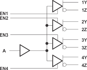
SN65LVDS105PWR 电路图
SN65LVDS105PWR 相关产品
- 29F52SC
- AD8016ARBZ
- AD8016ARBZ-REEL
- AD8016AREZ
- AD8016AREZ-REEL
- AD8016AREZ-REEL7
- AD8018ARUZ-REEL
- AD8018ARZ-REEL7
- AD807A-155BRZRL
- AD807A-155BRZRL7
- AD8128ACPZ-R7
- AD8145WYCPZ-R7
- AD8145YCPZ-R7
- AD8392AACPZ-RL
- AD8392AAREZ
- AD8392AAREZ-RL
- ADM1181AANZ
- ADM1385ARSZ-REEL
- ADM1385ARSZ-REEL7
- ADM1485ARMZ-REEL
- ADM1485ARMZ-REEL7
- ADM1485ARZ
- ADM1485JNZ
- ADM1486AR-REEL7
- ADM1486ARZ-REEL7
- ADM1490EBRMZ-REEL7
- ADM1490EBRZ
- ADM1490EBRZ-REEL7
- ADM202EARN-REEL
- ADM202EARNZ-REEL7