 搜索
搜索
 发布采购
发布采购
- 封装:16-TSSOP(0.173",4.40mm 宽)
- RoHS:无铅 / 符合限制有害物质指令(RoHS)规范要求
- 包装方式:带卷 (TR)
- 参考价格:$1.676
更新日期:2024-04-01 00:04:00

产品简介:双通道 LVDS 收发器
查看详情- 封装:16-TSSOP(0.173",4.40mm 宽)
- RoHS:无铅 / 符合限制有害物质指令(RoHS)规范要求
- 包装方式:带卷 (TR)
- 参考价格:$1.676
SN65LVDS050PWR 供应商
- 公司
- 型号
- 品牌
- 封装/批号
- 数量
- 地区
- 日期
- 说明
- 询价
-
TI
-
原厂原装
22+ -
3288
-
上海市
-
-
-
一级代理原装
-
TI(德州仪器)
-
TSSOP-16
2022+ -
12000
-
上海市
-
-
-
原装可开发票
SN65LVDS050PWR 中文资料属性参数
- 标准包装:2,000
- 类别:集成电路 (IC)
- 家庭:接口 - 驱动器,接收器,收发器
- 系列:65LVDS
- 类型:收发器
- 驱动器/接收器数:2/2
- 规程:LVDS
- 电源电压:3 V ~ 3.6 V
- 安装类型:表面贴装
- 封装/外壳:16-TSSOP(0.173",4.40mm 宽)
- 供应商设备封装:16-TSSOP
- 包装:带卷 (TR)
产品特性
- Meets or Exceeds the Requirements of ANSI TIA/EIA-644-1995 Standard
- Full-Duplex Signaling Rates up to 150 Mbps
- Bus-Pin ESD Exceeds 12 kV
- Operates From a Single 3.3-V Supply
- Low-Voltage Differential Signaling With Typical Output Voltages of 350 mV and a 100-Ω Load
- Propagation Delay Times Driver: 1.7 ns Typical Receiver: 3.7 ns Typical
- Driver: 1.7 ns Typical
- Receiver: 3.7 ns Typical
- Power Dissipation at 200 MHz Driver: 25 mW Typical Receiver: 60 mW Typical
- Driver: 25 mW Typical
- Receiver: 60 mW Typical
- LVTTL Input Levels Are 5-V Tolerant
- Receiver Maintains High Input Impedance With VCC < 1.5 V
- Receiver Has Open-Circuit Fail Safe
产品概述
The SN65LVDS179, SN65LVDS180, SN65LVDS050, and SN65LVDS051 devices are differential line
drivers and receivers that use low-voltage differential signaling (LVDS) to achieve signaling rates
as high as 400 Mbps. The TIA/EIA-644 standard-compliant electrical interface provides a minimum
differential output voltage magnitude of 247 mV into a 100-Ω load and receipt of 100-mV signals
with up to 1 V of ground potential difference between a transmitter and receiver.These devices offer various driver, receiver, and enabling combinations in
industry-standard footprints. Because these devices are intended for use in simplex or distributed
simplex bus structures, the driver enable function does not put the differential outputs into a
high-impedance state but rather disconnects the input and reduces the quiescent power used by the
device. For these functions with a high-impedance driver output, see the SN65LVDM series of
devices. All devices are characterized for operation from –40°C to 85°C.
SN65LVDS050PWR 数据手册
| 数据手册 | 说明 | 数量 | 操作 |
|---|---|---|---|
 SN65LVDS050PWR SN65LVDS050PWR
|
Dual LVDS Transmitter/Receiver 16-TSSOP |
27页,1.31M | 查看 |
|
SN65LVDS050PWRG4
|
Dual LVDS Transmitter/Receiver 16-TSSOP |
27页,1.31M | 查看 |
SN65LVDS050PWR 电路图
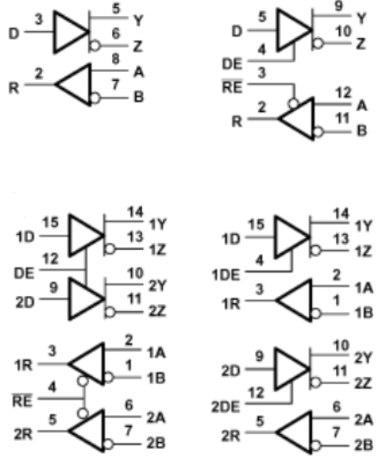
SN65LVDS050PWR 电路图
SN65LVDS050PWR 相关产品
- 29F52SC
- AD8016ARBZ
- AD8016ARBZ-REEL
- AD8016AREZ
- AD8016AREZ-REEL
- AD8016AREZ-REEL7
- AD8018ARUZ-REEL
- AD8018ARZ-REEL7
- AD807A-155BRZRL
- AD807A-155BRZRL7
- AD8128ACPZ-R7
- AD8145WYCPZ-R7
- AD8145YCPZ-R7
- AD8392AACPZ-RL
- AD8392AAREZ
- AD8392AAREZ-RL
- ADM1181AANZ
- ADM1385ARSZ-REEL
- ADM1385ARSZ-REEL7
- ADM1485ARMZ-REEL
- ADM1485ARMZ-REEL7
- ADM1485ARZ
- ADM1485JNZ
- ADM1486AR-REEL7
- ADM1486ARZ-REEL7
- ADM1490EBRMZ-REEL7
- ADM1490EBRZ
- ADM1490EBRZ-REEL7
- ADM202EARN-REEL
- ADM202EARNZ-REEL7