 搜索
搜索
 发布采购
发布采购
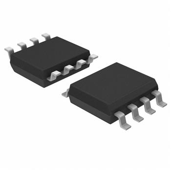
- 封装:8-SOIC(0.154",3.90mm 宽)
- RoHS:无铅 / 符合限制有害物质指令(RoHS)规范要求
- 包装方式:Digi-Reel®
- 参考价格:$3.168-$6.34
更新日期:2024-04-01 00:04:00
产品简介:具有故障保护功能的汽车类 70V RS-485 收发器
查看详情- 封装:8-SOIC(0.154",3.90mm 宽)
- RoHS:无铅 / 符合限制有害物质指令(RoHS)规范要求
- 包装方式:Digi-Reel®
- 参考价格:$3.168-$6.34
SN65HVD1781QDRQ1 供应商
- 公司
- 型号
- 品牌
- 封装/批号
- 数量
- 地区
- 日期
- 说明
- 询价
-
TI
-
SOIC-8
22+ -
2500
-
上海市
-
-
-
原厂原装上海仓现货
-
TI/德州仪器
-
21+
SOP8 -
10000
-
杭州
-
-
-
只做原装现货,大量现货热卖
-
TI(德州仪器)
-
SOIC-8
2022+ -
12000
-
上海市
-
-
-
原装可开发票
SN65HVD1781QDRQ1 中文资料属性参数
- 标准包装:1
- 类别:集成电路 (IC)
- 家庭:接口 - 驱动器,接收器,收发器
- 系列:-
- 类型:收发器
- 驱动器/接收器数:1/1
- 规程:RS485
- 电源电压:3.15 V ~ 5.5 V
- 安装类型:表面贴装
- 封装/外壳:8-SOIC(0.154",3.90mm 宽)
- 供应商设备封装:8-SOIC
- 包装:®
- 其它名称:296-27912-6
产品特性
- Qualified for Automotive Applications
- AEC-Q100 Qualified With the Following ResultsDevice Temperature Grade 1: –40°C to 125°C Ambient Operating Temperature RangeDevice HBM ESD Classification Level H2Device CDM ESG Classification Level C3B
- Device Temperature Grade 1: –40°C to 125°C Ambient Operating Temperature Range
- Device HBM ESD Classification Level H2
- Device CDM ESG Classification Level C3B
- Bus-Pin Fault Protection to:> ±70 V (’HVD1780-Q1, ’HVD1781-Q1)> ±30 V (’HVD1782-Q1)
- > ±70 V (’HVD1780-Q1, ’HVD1781-Q1)
- > ±30 V (’HVD1782-Q1)
- Operation With 3.3-V to 5-V Supply Range
- ±16-kV HBM Protection on Bus Pins
- Reduced Unit Load for up to 320 Nodes
- Failsafe Receiver for Open-Circuit, Short-Circuit and Idle-Bus Conditions
- Low Power Consumption Low Standby Supply Current, 1 µA Maximum ICC 4-mA Quiescent During Operation
- Low Standby Supply Current, 1 µA Maximum
- ICC 4-mA Quiescent During Operation
- Pin-Compatible With Industry-Standard SN75176
- Signaling Rates of 115 kbps, 1 Mbps, and up to 10 Mbps
产品概述
These devices are designed to survive overvoltage faults such as direct shorts to power
supplies, mis-wiring faults, connector failures, cable crushes, and tool mis-applications. They are
also robust to ESD events, with high levels of protection to the human-body-model
specification. These devices combine a differential driver and a differential receiver, which operate
from a single power supply. In the ’HVD1782, the driver differential outputs and the receiver
differential inputs are connected internally to form a bus port suitable for half-duplex (two-wire
bus) communication. This port features a wide common-mode voltage range, making the devices
suitable for multipoint applications over long cable runs. These devices are characterized from
–40°C to 125°C. These devices are pin-compatible with the industry-standard SN75176 transceiver,
making them drop-in upgrades in most systems. These devices are fully compliant with ANSI TIA/EIA 485-A with a 5-V supply and can
operate with a 3.3-V supply with reduced driver output voltage for low-power applications. For
applications where operation is required over an extended common-mode voltage range, see the
SN65HVD1785 (SLLS872) data sheet.
SN65HVD1781QDRQ1 电路图
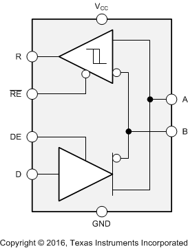
SN65HVD1781QDRQ1 电路图
SN65HVD1781QDRQ1 相关产品
- 29F52SC
- AD8016ARBZ
- AD8016ARBZ-REEL
- AD8016AREZ
- AD8016AREZ-REEL
- AD8016AREZ-REEL7
- AD8018ARUZ-REEL
- AD8018ARZ-REEL7
- AD807A-155BRZRL
- AD807A-155BRZRL7
- AD8128ACPZ-R7
- AD8145WYCPZ-R7
- AD8145YCPZ-R7
- AD8392AACPZ-RL
- AD8392AAREZ
- AD8392AAREZ-RL
- ADM1181AANZ
- ADM1385ARSZ-REEL
- ADM1385ARSZ-REEL7
- ADM1485ARMZ-REEL
- ADM1485ARMZ-REEL7
- ADM1485ARZ
- ADM1485JNZ
- ADM1486AR-REEL7
- ADM1486ARZ-REEL7
- ADM1490EBRMZ-REEL7
- ADM1490EBRZ
- ADM1490EBRZ-REEL7
- ADM202EARN-REEL
- ADM202EARNZ-REEL7