 搜索
搜索
 发布采购
发布采购
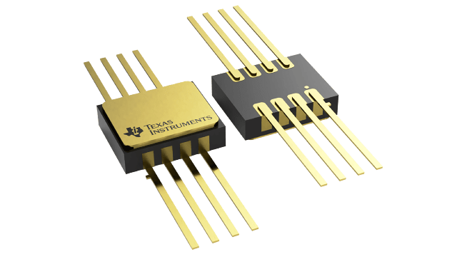
- 封装:8-CDFF
- RoHS:含铅 / 不符合限制有害物质指令(RoHS)规范要求
- 包装方式:管件
- 参考价格:$48-$66
更新日期:2024-04-01 00:04:00
产品简介:高温 3.3V RS-485 收发器
查看详情- 封装:8-CDFF
- RoHS:含铅 / 不符合限制有害物质指令(RoHS)规范要求
- 包装方式:管件
- 参考价格:$48-$66
SN65HVD11SHKJ 供应商
- 公司
- 型号
- 品牌
- 封装/批号
- 数量
- 地区
- 日期
- 说明
- 询价
-
TI
-
原厂原装
22+ -
3288
-
上海市
-
-
-
一级代理原装
-
TI(德州仪器)
-
CFP-8
2022+ -
12000
-
上海市
-
-
-
原装可开发票
SN65HVD11SHKJ 中文资料属性参数
- 标准包装:1
- 类别:集成电路 (IC)
- 家庭:接口 - 驱动器,接收器,收发器
- 系列:-
- 类型:收发器
- 驱动器/接收器数:1/1
- 规程:RS485
- 电源电压:3 V ~ 3.6 V
- 安装类型:表面贴装
- 封装/外壳:8-CDFF
- 供应商设备封装:8-CFP
- 包装:管件
- 其它名称:296-28287-5SN65HVD11SHKJ-ND
产品特性
- Operates With a 3.3-V Supply
- Bus-Pin ESD Protection Exceeds 16-kV Human- Body Model (HBM)
- 1/8 Unit-Load Option Available (up to 256 Nodes on Bus)
- Optional Driver Output Transition Times for Signaling Rates(1) of 1 Mbps, 10 Mbps, and 32 Mbps
- Based on ANSI TIA/EIA-485-A
- Bus-Pin Short Circuit Protection From –7 V to 12 V
- Open-Circuit, Idle-Bus, and Shorted-Bus Fail-Safe Receiver
- Glitch-Free Power-Up and Power-Down Protection for Hot-Plugging Applications
- SN75176 Footprint
- Supports Extreme Temperature Applications: Controlled Baselines One Assembly and Test Sites One Fabrication Sites Available in Extreme (–55°C/210°C) Temperature Range(2) Extended Product Life Cycles Extended Product-Change Notifications Product Traceability Texas Instruments’ High Temperature Products Use Highly Optimized Silicon (Die) Solutions With Design and Process Enhancements to Maximize Performance Over Extended Temperatures.
- Controlled Baselines
- One Assembly and Test Sites
- One Fabrication Sites
- Available in Extreme (–55°C/210°C) Temperature Range(2)
- Extended Product Life Cycles
- Extended Product-Change Notifications
- Product Traceability
- Texas Instruments’ High Temperature Products Use Highly Optimized Silicon (Die) Solutions With Design and Process Enhancements to Maximize Performance Over Extended Temperatures.
产品概述
The SN65HVD11-HT device combines a 3-state differential line driver and differential
input line receiver that operates with a single 3.3-V power supply. It is designed for balanced
transmission lines and meets or exceeds ANSI TIA/EIA-485-A and ISO 8482:1993, with the exception
that the thermal shutdown is removed. This differential bus transceiver is a monolithic integrated
circuit designed for bidirectional data communication on multipoint bus-transmission lines. The
driver and receiver have active-high and active-low enables, respectively, that can be externally
connected together to function as direction control.The driver differential outputs and receiver differential inputs connect internally to
form a differential input/ output (I/O) bus port that is designed to offer minimum loading to the
bus when the driver is disabled or VCC = 0.
SN65HVD11SHKJ 电路图
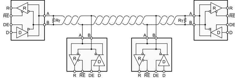
SN65HVD11SHKJ 电路图
SN65HVD11SHKJ 相关产品
- 29F52SC
- AD8016ARBZ
- AD8016ARBZ-REEL
- AD8016AREZ
- AD8016AREZ-REEL
- AD8016AREZ-REEL7
- AD8018ARUZ-REEL
- AD8018ARZ-REEL7
- AD807A-155BRZRL
- AD807A-155BRZRL7
- AD8128ACPZ-R7
- AD8145WYCPZ-R7
- AD8145YCPZ-R7
- AD8392AACPZ-RL
- AD8392AAREZ
- AD8392AAREZ-RL
- ADM1181AANZ
- ADM1385ARSZ-REEL
- ADM1385ARSZ-REEL7
- ADM1485ARMZ-REEL
- ADM1485ARMZ-REEL7
- ADM1485ARZ
- ADM1485JNZ
- ADM1486AR-REEL7
- ADM1486ARZ-REEL7
- ADM1490EBRMZ-REEL7
- ADM1490EBRZ
- ADM1490EBRZ-REEL7
- ADM202EARN-REEL
- ADM202EARNZ-REEL7