 搜索
搜索
 发布采购
发布采购
- 参考价格:¥4.28-¥4.83
更新日期:2024-04-01 00:04:00

SN65HVD1040DRG4 供应商
- 公司
- 型号
- 品牌
- 封装/批号
- 数量
- 地区
- 日期
- 说明
- 询价
-
TI
-
原厂原装
22+ -
3288
-
上海市
-
-
-
一级代理原装
-
TI
-
SOP-8
23+ -
5800
-
上海市
-
-
-
进口原装现货,杜绝假货。
SN65HVD1040DRG4 中文资料属性参数
- 制造商:Texas Instruments
- 产品种类:CAN 接口集成电路
- 封装 / 箱体:SOIC-8
- 封装:Reel
- 数据速率:1 Mbps
- 最大工作温度:+ 125 C
- 最小工作温度:- 40 C
- 安装风格:SMD/SMT
- 工厂包装数量:2500
产品特性
- Improved Drop-in Replacement for the TJA1040
- ±12 kV ESD Protection
- Low-Current Standby Mode With Bus Wakeup: 5 µA Typical
- Bus-Fault Protection of –27 V to 40 V
- Rugged Split-Pin Bus Stability
- Dominant Time-Out Function
- Power-Up/Down Glitch-Free Bus Inputs and Outputs High Input Impedance With Low VCC Monotonic Outputs During Power Cycling
- High Input Impedance With Low VCC
- Monotonic Outputs During Power Cycling
- DeviceNet™ Vendor ID Number 806
产品概述
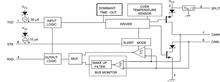
The SN65HVD1040 meets or exceeds the specifications of the ISO 11898 standard for use in
applications employing a Controller Area Network (CAN). As a CAN bus transceiver, the SN65HVD1040
device provides differential transmit and receive capability for a CAN controller at signaling
rates of up to 1 Mbps(1).Designed for operation in especially harsh environments, the device features ±12 kV ESD
protection on the bus and split pins, cross-wire, overvoltage and loss of ground protection from
–27 V to 40 V, overtemperature shutdown, a –12 V to 12 V common-mode range, and will withstanding
voltage transients from –200 V to 200 V according to ISO 7637.The STB input (pin 8) selects between two different modes of operation; high-speed or
low-power mode. The high-speed mode of operation is selected by connecting STB to ground.If a high logic level is applied to the STB pin of the SN65HVD1040, the device enters a
low-power bus-monitor standby mode. While the SN65HVD1040 is in the low-power bus-monitor standby
mode, a dominant bit greater than 5 μs on the bus is passed by the bus-monitor circuit to the
receiver output. The local protocol controller may then reactivate the device when it needs to
transmit to the bus.A dominant time-out circuit in the SN65HVD1040 prevents the driver from blocking network
communication during a hardware or software failure. The time-out circuit is triggered by a falling
edge on TXD (pin 1). If no rising edge is seen before the time-out constant of the circuit expires,
the driver is disabled. The circuit is then reset by the next rising edge on TXD.The SPLIT output (pin 5) is available on the SN65HVD1040 as a
VCC/2 common-mode bus voltage bias for a split-termination network.The SN65HVD1040 is characterized for operation from –40°C to 125°C.
SN65HVD1040DRG4 电路图
SN65HVD1040DRG4 电路图
SN65HVD1040DRG4 相关产品
- 100301QC
- 100304QC
- 100310QC
- 100311QC
- 100313QC
- 100316QC
- 100322QC
- 100329APC
- 100329DC
- 100336DC
- 100336PC
- 100341QC
- 100351DC
- 100351PC
- 100363QC
- 100364QC
- 100370QC
- 100390QC
- 100398QI
- 11AA010T-I/TT
- 11AA160T-I/TT
- 11LC010T-I/TT
- 11LC020T-I/TT
- 11LC040T-E/TT
- 11LC160T-E/TT
- 1ED020I12-F
- 2304NZGI-1LF
- 23A640-I/SN
- 23K256-I/SN
- 23K256-I/ST