 搜索
搜索
 发布采购
发布采购
- 封装:8-SOIC(0.154",3.90mm 宽)
- RoHS:无铅 / 符合限制有害物质指令(RoHS)规范要求
- 包装方式:Digi-Reel®
- 参考价格:$0.894-$1.91
更新日期:2024-04-01 00:04:00
产品简介:汽车类 EMC 优化 CAN 收发器
查看详情- 封装:8-SOIC(0.154",3.90mm 宽)
- RoHS:无铅 / 符合限制有害物质指令(RoHS)规范要求
- 包装方式:Digi-Reel®
- 参考价格:$0.894-$1.91
SN65HVD1040AQDRQ1 供应商
- 公司
- 型号
- 品牌
- 封装/批号
- 数量
- 地区
- 日期
- 说明
- 询价
-
TI
-
SOP8
21+ -
2500
-
上海市
-
-
-
原厂原装上海仓现货
-
TI
-
SMD
22+ -
50000
-
上海市
-
-
-
原装进口
-
TI/德州仪器
-
21+
SOP8 -
10000
-
杭州
-
-
-
只做原装现货,大量现货热卖
-
TI(德州仪器)
-
SOIC-8
2022+ -
9
-
上海市
-
-
-
原装可开发票
SN65HVD1040AQDRQ1 中文资料属性参数
- 标准包装:1
- 类别:集成电路 (IC)
- 家庭:接口 - 驱动器,接收器,收发器
- 系列:-
- 类型:收发器
- 驱动器/接收器数:1/1
- 规程:CAN
- 电源电压:4.75 V ~ 5.25 V
- 安装类型:表面贴装
- 封装/外壳:8-SOIC(0.154",3.90mm 宽)
- 供应商设备封装:8-SOIC
- 包装:®
- 其它名称:296-23668-6
产品特性
- Qualified for Automotive Applications
- AEC-Q100 Test Guidance With the Following: Device Temperature Grade 0: –40°C to +150°C Ambient Operating Temperature Device HBM ESD Classification Level: 3A Level for All Pins Except 5, 6, and 7 3B Level for Pins 5, 6 and 7 Device CDM ESD Classification Level C6 Device MM ESD Classification Level M3
- Device Temperature Grade 0: –40°C to +150°C Ambient Operating Temperature
- Device HBM ESD Classification Level: 3A Level for All Pins Except 5, 6, and 7 3B Level for Pins 5, 6 and 7
- Device CDM ESD Classification Level C6
- Device MM ESD Classification Level M3
- Improved Drop-In Replacement for TJA1040
- Meets or Exceeds the Requirements of ISO 11898-5
- GIFT/ICT Compliant
- ESD Protection up to ±12 kV (Human-Body Model) on Bus Pins
- Low-Current Standby Mode With Bus Wake-Up, <12 µA Maximum
- High Electromagnetic Compliance (EMC)
- Bus-Fault Protection of –27 V to 40 V
- Dominant Time-Out Function
- Thermal Shutdown Protection
- SPLIT Voltage Source for Common-Mode Stabilization of Bus Through Split Termination
- Digital Inputs Compatible With 3.3-V and 5-V Microprocessors.
- Power-Up and Power-Down Glitch-Free Bus Inputs and Outputs High Input Impedance With Low VCC Monotonic Outputs During Power Cycling
- High Input Impedance With Low VCC
- Monotonic Outputs During Power Cycling
- APPLICATIONS GMW3122 Dual-Wire CAN Physical Layers SAE J2284 High-Speed CAN for Automotive Applications SAE J1939 Standard Data Bus Interface ISO 11783 Standard Data Bus Interface NMEA 2000 Standard Data Bus Interface
- GMW3122 Dual-Wire CAN Physical Layers
- SAE J2284 High-Speed CAN for Automotive Applications
- SAE J1939 Standard Data Bus Interface
- ISO 11783 Standard Data Bus Interface
- NMEA 2000 Standard Data Bus Interface
产品概述
The SN65HVD1040A device meets or exceeds the specifications of the ISO 11898 standard for
use in applications employing a Controller Area Network (CAN). The device is qualified for use in
automotive applications.As a CAN transceiver, this device provides differential transmit capability to the bus
and differential receive capability to a CAN controller at signaling rates up to 1 megabit per
second (Mbps)(1).Designed for operation in especially harsh environments, the SN65HVD1040A-Q1 features
cross-wire, overvoltage, and loss of ground protection from –27 V to 40 V, overtemperature
protection, a –12-V to 12-V common-mode range, and can withstand voltage transients according to
ISO 7637.STB (pin 8) provides two different modes of operation: high-speed mode or low-current
standby mode. The high-speed mode of operation is selected by connecting STB (pin 8) to ground.If a high logic level is applied to the STB pin of the SN65HVD1040A-Q1, the device enters
a low-current standby mode, while the receiver remains active in a low-power bus-monitor standby
mode.In the low-current standby mode, a dominant bit greater than 5 µs on the bus is passed by
the bus-monitor circuit to the receiver output. The local protocol controller may then reactivate
the device when it needs to transmit to the bus.A dominant time-out circuit in the SN65HVD1040A-Q1 prevents the driver from blocking
network communication with a hardware or software failure. The time-out circuit is triggered by a
falling edge on TXD (pin 1). If no rising edge is seen before the time-out constant of the circuit
expires, the driver is disabled. The circuit is then reset by the next rising edge on TXD.SPLIT (pin 5) is available as a VCC/2 common-mode bus voltage bias
for a split-termination network (see Application and Implementation).
SN65HVD1040AQDRQ1 电路图
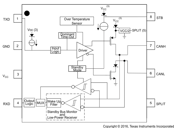
SN65HVD1040AQDRQ1 电路图
SN65HVD1040AQDRQ1 相关产品
- 29F52SC
- AD8016ARBZ
- AD8016ARBZ-REEL
- AD8016AREZ
- AD8016AREZ-REEL
- AD8016AREZ-REEL7
- AD8018ARUZ-REEL
- AD8018ARZ-REEL7
- AD807A-155BRZRL
- AD807A-155BRZRL7
- AD8128ACPZ-R7
- AD8145WYCPZ-R7
- AD8145YCPZ-R7
- AD8392AACPZ-RL
- AD8392AAREZ
- AD8392AAREZ-RL
- ADM1181AANZ
- ADM1385ARSZ-REEL
- ADM1385ARSZ-REEL7
- ADM1485ARMZ-REEL
- ADM1485ARMZ-REEL7
- ADM1485ARZ
- ADM1485JNZ
- ADM1486AR-REEL7
- ADM1486ARZ-REEL7
- ADM1490EBRMZ-REEL7
- ADM1490EBRZ
- ADM1490EBRZ-REEL7
- ADM202EARN-REEL
- ADM202EARNZ-REEL7