 搜索
搜索
 发布采购
发布采购
- 参考价格:RMB30.50-RMB52.50
更新日期:2024-04-01 00:04:00

产品简介:具有三态输出的军用 8 通道 4.5V 至 5.5V 双极缓冲器
查看详情- 参考价格:RMB30.50-RMB52.50
SN54LS244J 供应商
- 公司
- 型号
- 品牌
- 封装/批号
- 数量
- 地区
- 日期
- 说明
- 询价
-
TI
-
-
0 -
1000
-
杭州
-
-
-
原装正品现货
-
DIP
2019+ -
5800
-
上海市
-
-
-
全新原装现货
-
TI
-
模块
23+ -
15000
-
上海市
-
-
-
中国区代理原装进口特价
-
TI
-
-
21+ -
8000
-
上海市
-
-
-
原装现货,品质为先!请来电垂询!
-
TI
-
CDIP
23+ -
5800
-
上海市
-
-
-
进口原装现货,杜绝假货。
-
TI
-
DIP
- -
69
-
台州
-
-
-
自己现货,深圳可交易
SN54LS244J 中文资料属性参数
- 传输延迟测试条件:45pF
- 安装类型:通孔
- 宽度:6.92mm
- 封装类型:CDIP
- 尺寸:24.2 x 6.92 x 4.57mm
- 引脚数目:20
- 最低工作温度:-55 °C
- 最大低电平输出电流:12mA
- 最大工作电源电压:5.5 V
- 最大高电平输出电流:-12mA
- 最小工作电源电压:4.5 V
- 最长传播延迟时间@最长CL:18 ns @ 5 V
- 最高工作温度:+125 °C
- 极性:非反相
- 每片芯片通道数目:8
- 输入类型:单端
- 输出类型:三态
- 逻辑功能:缓冲器,线路驱动器
- 逻辑系列:LS
- 长度:24.2mm
- 高度:4.57mm
产品特性
- Inputs Tolerant Down to 2 V, Compatible With 3.3-V or 2.5-V Logic Inputs
- Maximum tpd of 15 ns at 5 V
- 3-State Outputs Drive Bus Lines or Buffer Memory Address Registers
- PNP Inputs Reduce DC Loading
- Hysteresis at Inputs Improves Noise Margins
产品概述
The SNx4LS24x, SNx4S24x octal buffers and line drivers are designed specifically to
improve both the performance and density of three-state memory address drivers, clock drivers, and
bus-oriented receivers and transmitters. The designer has a choice of selected combinations of
inverting and non-inverting outputs, symmetrical, active-low output-control
(G) inputs, and complementary output-control (G and
G) inputs. These devices feature high fan-out, improved fan-in, and 400-mV
noise margin. The SN74LS24x and SN74S24x devices can be used to drive terminated lines down to 133
Ω.
SN54LS244J 电路图
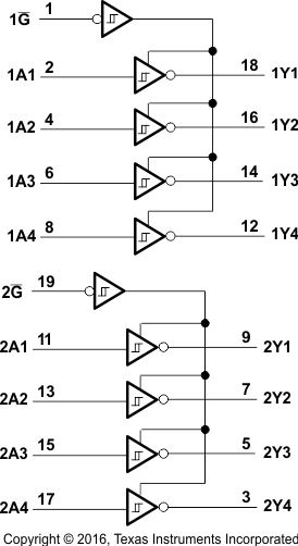
SN54LS244J 电路图