 搜索
搜索
 发布采购
发布采购
更新日期:2024-04-01 00:04:00

产品简介:具有 15V 容限集电极开路输出的军用六通道、4.5V 至 5.5V 双极性缓冲器
查看详情SN5417J 供应商
- 公司
- 型号
- 品牌
- 封装/批号
- 数量
- 地区
- 日期
- 说明
- 询价
-
TI
-
-
8 -
5500
-
杭州
-
-
-
原装正品现货
-
TI
-
CDIP
23+ -
5800
-
上海市
-
-
-
进口原装现货,杜绝假货。
-
TI
-
DIP
- -
41
-
台州
-
-
SN5417J 中文资料属性参数
- 现有数量:0现货1,638Factory
- 价格:在售
- 系列:*
- 包装:管件
- 产品状态:在售
- 逻辑类型:-
- 元件数:-
- 每个元件位数:-
- 输入类型:-
- 输出类型:-
- 电流 - 输出高、低:-
- 电压 - 供电:-
- 工作温度:-
- 安装类型:-
- 封装/外壳:-
- 供应商器件封装:-
产品特性
- Convert TTL Voltage Levels to MOS Levels
- High Sink-Current Capability Design
- Open-Collector Driver for Indicator Lamps
- Inputs Fully Compatible With Most TTL Circuits
- On Products Compliant to MIL-PRF-38535, All Parameters Are Tested Unless Otherwise Noted. On All Other Products, Production Processing Does Not Necessarily Include Testing of All Parameters.
产品概述
These TTL hex buffers and drivers feature high-voltage open-collector outputs for
interfacing with high-level circuits (such as MOS) or for driving high-current loads (such as lamps
or relays), and also are characterized for use as buffers for driving TTL inputs. The SN5407 and
SN7407 devices have minimum breakdown voltages of 30 V, and the SN5417 and SN7417 devices have
minimum breakdown voltages of 15 V. The maximum sink current is 30 mA for the SN5407 and SN5417
devices and 40 mA for the SN7407 and SN7417 devices.These devices perform the Boolean function Y = A in positive logic.These circuits are completely compatible with most TTL families. Inputs are diode clamped
to minimize transmission-line effects, which simplifies design. Typical power dissipation is 145
mW, and average propagation delay time is 14 ns.
SN5417J 数据手册
 SN5417J
SN5417J 电路图
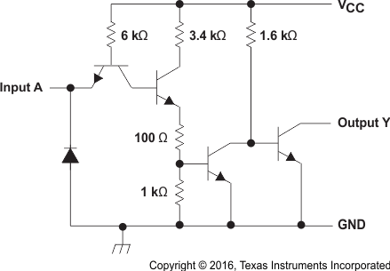
SN5417J 电路图
SN5417J 相关产品
- 1P1G125QDRYRQ1
- 1P1G126QDRYRQ1
- 1P2GU04QDRYRQ1
- 2N7001TDCKR
- 2N7001TDPWR
- 54FCT245TDB
- 5962-8762401CA
- 5962-8766301MRA
- 5962-8768001EA
- 7202LA50JG
- 7203L20TDB
- 7204L35J
- 72805LB15PF
- 7280L20PA
- 72V201L15PFGI
- 72V211L10PFG
- 72V245L10PFG
- 72V3640L10PF
- 72V3660L7-5PFI
- 72V70210DAG
- 72V70840DAG
- 72V73273BBG
- 74AHC05S14-13
- 74AHC05T14-13
- 74AHC1G126MDCKTEP
- 74AHC32S14-13
- 74AHC594S16-13
- 74AHC594T16-13
- 74AHCT08PW-Q100J
- 74AHCT125S14-13