 搜索
搜索
 发布采购
发布采购
- 参考价格:¥2,652.29-¥2,801.47
更新日期:2024-04-01 00:04:00

产品简介:具有 150MHz 频率、256kB 闪存、EMIF 的 C2000? 增强型产品 32 位 MCU
查看详情- 参考价格:¥2,652.29-¥2,801.47
SM320F2812HFGM150 供应商
- 公司
- 型号
- 品牌
- 封装/批号
- 数量
- 地区
- 日期
- 说明
- 询价
-
TI
-
CFPAK-172
21+ -
800
-
上海市
-
-
-
原装现货,品质为先!请来电垂询!
-
TI
-
CQFP
16+ -
2
-
台州
-
-
-
TI
-
-
最新批号 -
6996
-
上海市
-
-
SM320F2812HFGM150 中文资料属性参数
- 制造商:Texas Instruments
- 产品种类:数字信号处理器与控制器 (DSP, DSC)
- 数据总线宽度:32 bit
- 程序存储器大小:1 K
- 数据 RAM 大小:36 KB
- 最大时钟频率:150 MHz
- 可编程输入/输出端数量:56
- 工作电源电压:1.9 V
- 最大工作温度:+ 125 C
- 封装 / 箱体:CFP-172
- 安装风格:SMD/SMT
- 最小工作温度:- 55 C
- 产品:DSPs
- 程序存储器类型:OTP ROM
- 工厂包装数量:1
产品特性
- High-Performance Static CMOS Technology 150 MHz (6.67-ns Cycle Time) Low-Power (1.8-V Core at 135 MHz, 1.9-V Core at 150 MHz, 3.3-V I/O) Design 3.3-V Flash Voltage
- 150 MHz (6.67-ns Cycle Time)
- Low-Power (1.8-V Core at 135 MHz, 1.9-V Core at 150 MHz, 3.3-V I/O) Design
- 3.3-V Flash Voltage
- JTAG Boundary Scan Support
- High-Performance 32-Bit CPU (TMS320C28x) 16 x 16 and 32 x 32 MAC Operations 16 x 16 Dual MAC Harvard Bus Architecture Atomic Operations Fast Interrupt Response and Processing Unified Memory Programming Model 4M Linear Program Address Reach 4M Linear Data Address Reach Code-Efficient (in C/C++ and Assembly) TMS320F24x/LF240x Processor Source Code Compatible
- 16 x 16 and 32 x 32 MAC Operations
- 16 x 16 Dual MAC
- Harvard Bus Architecture
- Atomic Operations
- Fast Interrupt Response and Processing
- Unified Memory Programming Model
- 4M Linear Program Address Reach
- 4M Linear Data Address Reach
- Code-Efficient (in C/C++ and Assembly)
- TMS320F24x/LF240x Processor Source Code Compatible
- On-Chip Memory Flash Devices: Up to 128K x 16 Flash (Four 8K x 16 and Six 16K x 16 Sectors) ROM Devices: Up to 128K x 16 ROM 1K x 16 OTP ROM L0 and L1: 2 Blocks of 4K x 16 Each Single-Access RAM (SARAM) H0: 1 Block of 8K x 16 SARAM M0 and M1: 2 Blocks of 1K x 16 Each SARAM
- Flash Devices: Up to 128K x 16 Flash (Four 8K x 16 and Six 16K x 16 Sectors)
- ROM Devices: Up to 128K x 16 ROM
- 1K x 16 OTP ROM
- L0 and L1: 2 Blocks of 4K x 16 Each Single-Access RAM (SARAM)
- H0: 1 Block of 8K x 16 SARAM
- M0 and M1: 2 Blocks of 1K x 16 Each SARAM
- Boot ROM (4K x 16) With Software Boot Modes Standard Math Tables
- With Software Boot Modes
- Standard Math Tables
- External Interface Up to 1M Total Memory Programmable Wait States Programmable Read/Write Strobe Timing Three Individual Chip Selects
- Up to 1M Total Memory
- Programmable Wait States
- Programmable Read/Write Strobe Timing
- Three Individual Chip Selects
- Clock and System Control Dynamic PLL Ratio Changes Supported On-Chip Oscillator Watchdog Timer Module
- Dynamic PLL Ratio Changes Supported
- On-Chip Oscillator
- Watchdog Timer Module
- Three External Interrupts
- Peripheral Interrupt Expansion (PIE) Block That Supports 45 Peripheral Interrupts
- 128-Bit Security Key/Lock Protects Flash/ROM/OTP and L0/L1 SARAM Prevents Firmware Reverse Engineering
- Protects Flash/ROM/OTP and L0/L1 SARAM
- Prevents Firmware Reverse Engineering
- Three 32-Bit CPU-Timers
- Motor Control Peripherals Two Event Managers (EVA, EVB) Compatible to 240xA Devices
- Two Event Managers (EVA, EVB)
- Compatible to 240xA Devices
- Serial Port Peripherals Serial Peripheral Interface (SPI) Two Serial Communications Interfaces (SCIs), Standard UART Enhanced Controller Area Network (eCAN) Multichannel Buffered Serial Port (McBSP) With SPI Mode
- Serial Peripheral Interface (SPI)
- Two Serial Communications Interfaces (SCIs), Standard UART
- Enhanced Controller Area Network (eCAN)
- Multichannel Buffered Serial Port (McBSP) With SPI Mode
- 12-Bit ADC, 16 Channels 2 x 8 Channel Input Multiplexer Two Sample-and-Hold Single/Simultaneous Conversions Fast Conversion Rate: 80 ns/12.5 MSPS
- 2 x 8 Channel Input Multiplexer
- Two Sample-and-Hold
- Single/Simultaneous Conversions
- Fast Conversion Rate: 80 ns/12.5 MSPS
- Up to 56 Individually Programmable, Multiplexed General-Purpose Input/Output (GPIO) Pins
- Advanced Emulation Features Analysis and Breakpoint Functions Real-Time Debug via Hardware
- Analysis and Breakpoint Functions
- Real-Time Debug via Hardware
- Development Tools Include ANSI C/C++ Compiler/Assembler/Linker Supports TMS320C24x™/240x Instructions Code Composer Studio™ IDE DSP/BIOS™ JTAG Scan Controllers [Texas Instruments (TI) or Third-Party] Evaluation Modules Broad Third-Party Digital Motor Control Support
- ANSI C/C++ Compiler/Assembler/Linker
- Supports TMS320C24x™/240x Instructions
- Code Composer Studio™ IDE
- DSP/BIOS™
- JTAG Scan Controllers [Texas Instruments (TI) or Third-Party]
- Evaluation Modules
- Broad Third-Party Digital Motor Control Support
- Low-Power Modes and Power Savings IDLE, STANDBY, HALT Modes Supported Disable Individual Peripheral Clocks
- IDLE, STANDBY, HALT Modes Supported
- Disable Individual Peripheral Clocks
- Package Options 172-Pin Ceramic Quad Flatpack (HFG)
- 172-Pin Ceramic Quad Flatpack (HFG)
- Temperature Options: M: –55°C to 125°C (HFG)
- M: –55°C to 125°C (HFG)
产品概述
The SM320F2812 device, member of the C28x™ DSP generation, is a highly integrated, high-performance solution for demanding control applications. The functional blocks and the memory maps are described in Section 3, Functional Overview.Throughout this document, SM320F2812 is abbreviated as F2812.
SM320F2812HFGM150 电路图
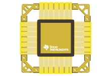
SM320F2812HFGM150 电路图
SM320F2812HFGM150 相关产品
- 100301QC
- 100304QC
- 100310QC
- 100311QC
- 100313QC
- 100316QC
- 100322QC
- 100329APC
- 100329DC
- 100336DC
- 100336PC
- 100341QC
- 100351DC
- 100351PC
- 100363QC
- 100364QC
- 100370QC
- 100390QC
- 100398QI
- 11AA010T-I/TT
- 11AA160T-I/TT
- 11LC010T-I/TT
- 11LC020T-I/TT
- 11LC040T-E/TT
- 11LC160T-E/TT
- 1ED020I12-F
- 2304NZGI-1LF
- 23A640-I/SN
- 23K256-I/SN
- 23K256-I/ST