 搜索
搜索
 发布采购
发布采购
- 参考价格:¥37.33-¥48.78
更新日期:2024-04-01 00:04:00

SCAN92LV090SLC 供应商
- 公司
- 型号
- 品牌
- 封装/批号
- 数量
- 地区
- 日期
- 说明
- 询价
-
TI
-
原厂原装
22+ -
3288
-
上海市
-
-
-
一级代理原装
SCAN92LV090SLC 中文资料属性参数
- 制造商:National Semiconductor (TI)
- 激励器数量:2
- 接收机数量:2
- 数据速率:100 Mbps
- 工作电源电压:3.3 V
- 最大功率耗散:1740 mW
- 最大工作温度:+ 85 C
- 封装 / 箱体:FBGA
- 封装:Tray
- 最小工作温度:- 40 C
- 安装风格:SMD/SMT
- 传播延迟时间:3.9 ns
- 工厂包装数量:360
- Supply Voltage - Max:3.6 V
- Supply Voltage - Min:3 V
- 类型:LVCMOS, LVTTL, LVDS
产品特性
- IEEE 1149.1 (JTAG) Compliant
- Bus LVDS Signaling
- Low Power CMOS Design
- High Signaling Rate Capability (Above 100 Mbps)
- 0.1V to 2.3V Common Mode Range for VID = 200mV
- ±100 mV Receiver Sensitivity
- Supports Open and Terminated Failsafe on Port Pins
- 3.3V Operation
- Glitch Free Power Up/Down (Driver & Receiver Disabled)
- Light Bus Loading (5 pF Typical) per Bus LVDS Load
- Designed for Double Termination Applications
- Balanced Output Impedance
- Product Offered in 64 Pin LQFP Package and NFBGA Package
- High Impedance Bus Pins on Power Off (VCC = 0V)
产品概述
The SCAN92LV090A is one in a series of Bus LVDS transceivers designed specifically for
the high speed, low power proprietary backplane or cable interfaces. The device operates from a
single 3.3V power supply and includes nine differential line drivers and nine receivers. To
minimize bus loading, the driver outputs and receiver inputs are internally connected. The separate
I/O of the logic side allows for loop back support. The device also features a flow through pin out
which allows easy PCB routing for short stubs between its pins and the connector.The driver translates 3V TTL levels (single-ended) to differential Bus LVDS (BLVDS)
output levels. This allows for high speed operation, while consuming minimal power with reduced
EMI. In addition, the differential signaling provides common mode noise rejection of ±1V.The receiver threshold is less than ±100 mV over a ±1V common mode range and translates
the differential Bus LVDS to standard (TTL/CMOS) levels.This device is compliant with IEEE 1149.1 Standard Test Access Port and Boundary Scan
Architecture with the incorporation of the defined boundary-scan test logic and test access port
consisting of Test Data Input (TDI), Test Data Out (TDO), Test Mode Select (TMS), Test Clock (TCK),
and the optional Test Reset (TRST).
SCAN92LV090SLC 数据手册
| 数据手册 | 说明 | 数量 | 操作 |
|---|---|---|---|
 SCAN92LV090SLC SCAN92LV090SLC
|
9 Channel Bus LVDS Transceiver w/ Boundary SCAN |
13 Pages页,693K | 查看 |
SCAN92LV090SLC 电路图
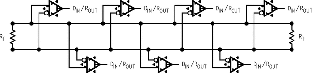
SCAN92LV090SLC 电路图
SCAN92LV090SLC 相关产品
- 100301QC
- 100304QC
- 100310QC
- 100311QC
- 100313QC
- 100316QC
- 100322QC
- 100329APC
- 100329DC
- 100336DC
- 100336PC
- 100341QC
- 100351DC
- 100351PC
- 100363QC
- 100364QC
- 100370QC
- 100390QC
- 100398QI
- 11AA010T-I/TT
- 11AA160T-I/TT
- 11LC010T-I/TT
- 11LC020T-I/TT
- 11LC040T-E/TT
- 11LC160T-E/TT
- 1ED020I12-F
- 2304NZGI-1LF
- 23A640-I/SN
- 23K256-I/SN
- 23K256-I/ST