 搜索
搜索
 发布采购
发布采购
- 参考价格:¥24.98-¥48.16
更新日期:2024-04-01 00:04:00

产品简介:具有预加重功能和 IEEE 1149.6 的 1.5Gbps 2x2 LVDS 交叉点开关
查看详情- 参考价格:¥24.98-¥48.16
SCAN90CP02VY/NOPB 供应商
- 公司
- 型号
- 品牌
- 封装/批号
- 数量
- 地区
- 日期
- 说明
- 询价
-
TI
-
原厂原装
22+ -
3288
-
上海市
-
-
-
一级代理原装
SCAN90CP02VY/NOPB 中文资料属性参数
- 制造商:National Semiconductor (TI)
- 封装 / 箱体:LQFP-32
- 数据速率:1.5 Gbps
- 输入电平:LVDS, BLVDS, CML, LVPECL
- 输出电平:LDVS
- Supply Voltage - Max:3.6 V
- Supply Voltage - Min:3 V
- 最大工作温度:+ 85 C
- 最小工作温度:- 40 C
- 产品:LVDS Crosspoint Switch
- 封装:Tray
- 安装风格:SMD/SMT
- 阵列数量:1
- 工作电源电压:3.3 V
- 工厂包装数量:250
- 电源类型:Digital
- 类型:2 x 2
产品特性
- 1.5 Gbps per Channel
- Low Power: 70 mA in Dual Repeater Mode @1.5 Gbps
- Low Output Jitter
- Configurable 0/25/50/100% Pre-Emphasis Drives Lossy Backplanes and Cables
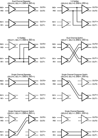
- Non-Blocking Architecture Allows 1:2 Splitter, 2:1 Mux, Crossover, and Dual Buffer Configurations
- Flow-Through Pinout
- LVDS/BLVDS/CML/LVPECL Inputs, LVDS Outputs
- IEEE 1149.1 and 1149.6 Compliant
- Single 3.3V Supply
- Separate Control of Inputs and Outputs Allows for Power Savings
- Industrial -40 to +85°C Temperature Range
- 28-Lead UQFN Package, or 32-Lead LQFP Package
产品概述
The SCAN90CP02 is a 1.5 Gbps 2 x 2 LVDS crosspoint switch. High speed data paths and
flow-through pinout minimize internal device jitter, while configurable 0/25/50/100% pre-emphasis
overcomes external ISI jitter effects of lossy backplanes and cables. The differential inputs
interface to LVDS and Bus LVDS signals such as those on TI's 10-, 16-, and 18- bit Bus LVDS SerDes,
as well as CML and LVPECL. The SCAN90CP02 can also be used with ASICs and FPGAs. The non-blocking
crosspoint architecture is pin-configurable as a 1:2 clock or data splitter, 2:1 redundancy mux,
crossover function, or dual buffer for signal booster and stub hider applications.Integrated IEEE 1149.1 (JTAG) and 1149.6 circuitry supports testability of both
single-ended LVTTL/CMOS and differential LVDS PCB interconnect. The 3.3V supply, CMOS process, and
LVDS I/O ensure high performance at low power over the entire industrial -40 to +85°C temperature
range.
SCAN90CP02VY/NOPB 数据手册
| 数据手册 | 说明 | 数量 | 操作 |
|---|---|---|---|
 SCAN90CP02VY/NOPB SCAN90CP02VY/NOPB
|
Crosspoint Switch; Supply Voltage Min:3V; Supply Voltage Max:3.6V; Termination Type:Solder; Package/Case:32-LQFP; No. of Pins:32; Operating Temperature Range:-40°C to +85°C; Leaded Process Compatible:Yes ;RoHS Compliant: Yes |
16页,354K | 查看 |
|
SCAN90CP02VY/NOPB
|
Crosspoint Switch 1 x 2:2 32-TQFP (7x7) |
22页,1.11M | 查看 |
SCAN90CP02VY/NOPB 电路图
SCAN90CP02VY/NOPB 电路图
SCAN90CP02VY/NOPB 相关产品
- 100301QC
- 100304QC
- 100310QC
- 100311QC
- 100313QC
- 100316QC
- 100322QC
- 100329APC
- 100329DC
- 100336DC
- 100336PC
- 100341QC
- 100351DC
- 100351PC
- 100363QC
- 100364QC
- 100370QC
- 100390QC
- 100398QI
- 11AA010T-I/TT
- 11AA160T-I/TT
- 11LC010T-I/TT
- 11LC020T-I/TT
- 11LC040T-E/TT
- 11LC160T-E/TT
- 1ED020I12-F
- 2304NZGI-1LF
- 23A640-I/SN
- 23K256-I/SN
- 23K256-I/ST