 搜索
搜索
 发布采购
发布采购
- 封装:10-TFSOP,10-MSOP(0.118",3.00mm 宽)
- RoHS:无铅 / 符合限制有害物质指令(RoHS)规范要求
- 包装方式:带卷 (TR)
- 参考价格:$2.081
更新日期:2024-04-01 00:04:00
产品简介:具有可编程增益和偏移的单电源自动置零传感器放大器
查看详情- 封装:10-TFSOP,10-MSOP(0.118",3.00mm 宽)
- RoHS:无铅 / 符合限制有害物质指令(RoHS)规范要求
- 包装方式:带卷 (TR)
- 参考价格:$2.081
PGA308AIDGSR 供应商
- 公司
- 型号
- 品牌
- 封装/批号
- 数量
- 地区
- 日期
- 说明
- 询价
-
TI
-
原厂原装
22+ -
3288
-
上海市
-
-
-
一级代理原装
-
TI/德州仪器
-
SC70-5
2024 -
91752
-
上海市
-
-
-
上海原装现货库存,欢迎咨询合作
-
TI
-
VSSOP-10
24+ -
5000
-
上海市
-
-
-
上海现货
-
Texas Instruments
-
原厂原装
22+授权代理 -
15800
-
上海市
-
-
-
旋尔只做进口原装,假一赔十...
-
TI(德州仪器)
-
VSSOP-10
2022+ -
4
-
上海市
-
-
-
原装可开发票
-
TI
-
PDIP (N)
23+ -
15000
-
上海市
-
-
-
中国区代理原装现货热卖特价
-
TI
-
MSOP10
新批号 -
8887770
-
上海市
-
-
-
原厂发货进口原装微信同步QQ893727827
-
TI
-
MSOP-10
23+ -
5800
-
上海市
-
-
-
进口原装现货,杜绝假货。
PGA308AIDGSR 中文资料属性参数
- 标准包装:2,500
- 类别:集成电路 (IC)
- 家庭:接口 - 传感器和探测器接口
- 系列:-
- 类型:信号调节器
- 输入类型:电压
- 输出类型:电压
- 接口:UART
- 电流 - 电源:-
- 安装类型:表面贴装
- 封装/外壳:10-TFSOP,10-MSOP(0.118",3.00mm 宽)
- 供应商设备封装:10-MSOP
- 包装:带卷 (TR)
产品特性
- Digital Calibration for Bridge Sensors
- Offset Select: Coarse and Fine
- Gain Select: Coarse and Fine
- Bridge Fault Monitor
- Input Mux for Lead Swap
- Over/Under Scale Limits
- DOUT/VOUT Clamp Function
- Seven Banks OTP Memory
- One-Wire Digital UART Interface
- Operating Voltage: +2.7V to +5.5V
- Temperature Range: –40°C to +125°C
- MSOP-10 and 3mm × 4mm DFN-10 Packages
产品概述
The PGA308 is a programmable analog sensor signal conditioner. The analog signal path amplifies the sensor signal and provides digital calibration for offset and gain. Calibration is done via the 1W pin, a digital One-Wire, UART-compatible interface. For three-terminal sensor modules, 1W may be connected to VOUT and the assembly programmed through the VOUT pin. Gain and offset calibration parameters are stored onboard in seven banks of one-time programmable (OTP) memory. The power-on reset (POR) OTP bank may be programmed a total of four times.The all-analog signal path contains a 2×2 input multiplexer (mux) to allow electronic sensor lead swapping, a coarse offset adjust, an auto-zero programmable gain instrumentation amplifier (PGA), a fine gain adjust, a fine offset adjust, and a programmable gain output amplifier. Fault monitor circuitry detects and signals sensor burnout, overload, and system fault conditions. Over/under-scale limits provide additional means for system level diagnostics. The dual-use DOUT/VCLAMP pin can be used as a programmable digital output or as a VOUT over-voltage clamp.For detailed application information, see the PGA308 User's Guide (SBOU069) available for download at www.ti.com.
PGA308AIDGSR 电路图
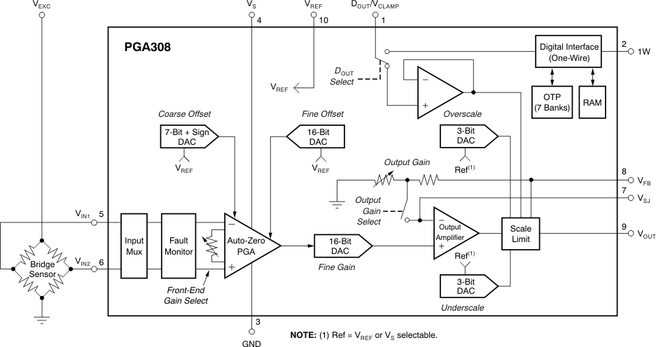
PGA308AIDGSR 电路图
PGA308AIDGSR 相关产品
- 1B31AN
- 1B32AN
- 1B41AN
- 1B41BN
- 1B51AN
- 1B51BN
- AD22050NZ
- AD22050RZ
- AD22050RZ-REEL
- AD22050RZ-REEL7
- AD22057RZ
- AD22057RZ-RL
- AD2S82AHP-REEL
- AD2S82AHPZ-REEL
- AD2S82ALPZ
- AD2S83APZ
- AD2S90APZ
- AD694ARZ
- AD694ARZ-REEL
- AD694BRZ-REEL
- AD694BRZ-REEL7
- AD698APZ
- AD7143ACPZ-1REEL
- AD80066KRSZ
- AD8494ARMZ
- AD8494ARMZ-R7
- AD8494CRMZ-R7
- AD8495ARMZ
- AD8495ARMZ-R7
- AD8495CRMZ