 搜索
搜索
 发布采购
发布采购
- 封装:20-TSSOP(0.173",4.40mm 宽)
- RoHS:无铅 / 符合限制有害物质指令(RoHS)规范要求
- 包装方式:管件
- 参考价格:$2.53125-$5.67
更新日期:2024-04-01 00:04:00

产品简介:具有 10 通道多路复用器的零温漂、100µV 失调电压、12nV/√Hz 噪声、RRO(二进制增益)可编程增益放大器
查看详情- 封装:20-TSSOP(0.173",4.40mm 宽)
- RoHS:无铅 / 符合限制有害物质指令(RoHS)规范要求
- 包装方式:管件
- 参考价格:$2.53125-$5.67
PGA116AIPW 供应商
- 公司
- 型号
- 品牌
- 封装/批号
- 数量
- 地区
- 日期
- 说明
- 询价
-
TI
-
原厂原装
22+ -
3288
-
上海市
-
-
-
一级代理原装
-
TI(德州仪器)
-
TSSOP-20
2022+ -
12000
-
上海市
-
-
-
原装可开发票
-
TI/德州仪器
-
TSSOP20
21+ -
10000
-
杭州
-
-
-
原装正品,BOM一站式服务
PGA116AIPW 中文资料属性参数
- 标准包装:70
- 类别:集成电路 (IC)
- 家庭:Linear - Amplifiers - Instrumentation, OP Amps, Buffer Amps
- 系列:-
- 放大器类型:可编程增益
- 电路数:1
- 输出类型:满摆幅
- 转换速率:8 V/µs
- 增益带宽积:-
- -3db带宽:10MHz
- 电流 - 输入偏压:1.5nA
- 电压 - 输入偏移:75µV
- 电流 - 电源:330µA
- 电流 - 输出 / 通道:60mA
- 电压 - 电源,单路/双路(±):2.2 V ~ 5.5 V
- 工作温度:-40°C ~ 125°C
- 安装类型:表面贴装
- 封装/外壳:20-TSSOP(0.173",4.40mm 宽)
- 供应商设备封装:20-TSSOP
- 包装:管件
- 其它名称:296-33535-5PGA116AIPW-ND
产品特性
- Rail-to-Rail Input and Output
- Offset: 25 µV (Typical), 100 µV (Maximum)
- Zerø Drift: 0.35 µV/°C (Typical), 1.2 µV/°C (Maximum)
- Low Noise: 12 nV/√Hz
- Input Offset Current: ±5 nA Maximum (25°C)
- Gain Error: 0.1% Maximum (G ≥ 32), 0.3% Maximum (G > 32)
- Binary Gains: 1, 2, 4, 8, 16, 32, 64, 128 (PGA112, PGA116)
- Scope Gains: 1, 2, 5, 10, 20, 50, 100, 200 (PGA113, PGA117)
- Gain Switching Time: 200 ns
- 2 Channel MUX: PGA112, PGA113 10 Channel MUX: PGA116, PGA117
- Four Internal Calibration Channels
- Amplifier Optimized for Driving CDAC ADCs
- Output Swing: 50 mV to Supply Rails
- AVDD and DVDD for Mixed Voltage Systems
- IQ = 1.1 mA (Typical)
- Software and Hardware Shutdown: IQ ≤ 4 µA (Typical)
- Temperature Range: –40°C to 125°C
- SPI™ Interface (10 MHz) With Daisy-Chain Capability
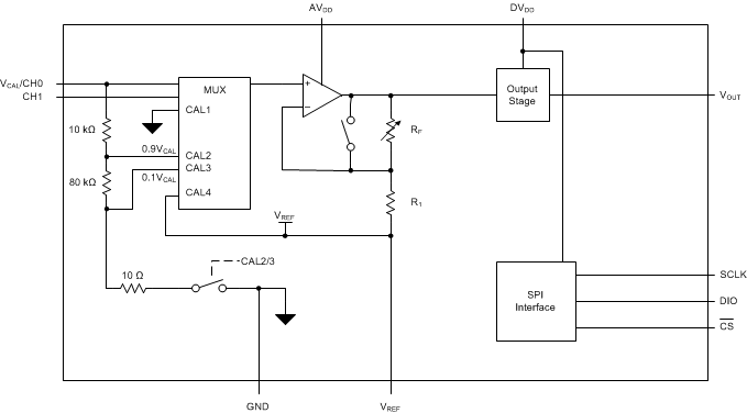
产品概述
The PGA112 and PGA113 devices (binary and scope gains) offer two analog inputs, a
three-pin SPI interface, and software shutdown in a 10-pin, VSSOP package. The PGA116 and PGA117
(binary and scope gains) offer 10 analog inputs, a SPI interface with daisy-chain capability, and
hardware and software shutdown in a 20-pin TSSOP package.All versions provide internal calibration channels for system-level calibration. The
channels are tied to GND, 0.9 VCAL, 0.1 VCAL, and
VREF, respectively. VCAL, an external voltage
connected to Channel 0, is used as the system calibration reference. Binary gains are: 1, 2, 4, 8,
16, 32, 64, and 128; scope gains are: 1, 2, 5, 10, 20, 50, 100, and 200.
PGA116AIPW 数据手册
| 数据手册 | 说明 | 数量 | 操作 |
|---|---|---|---|
 PGA116AIPW PGA116AIPW
|
Zero-Drift, Programmable Gain Amplifier with MUX 20-TSSOP -40 to 125 |
47页,1.55M | 查看 |
|
PGA116AIPW
|
Programmable Gain Amplifier 1 Circuit Rail-to-Rail 20-TSSOP |
49页,1.95M | 查看 |
PGA116AIPW 电路图
PGA116AIPW 电路图
PGA116AIPW 相关产品
- ACPL-7900-000E
- ACPL-7900-300E
- ACPL-790A-000E
- ACPL-790B-000E
- ACPL-790B-300E
- ACPL-C784-000E
- ACPL-C790-500E
- ACPL-C79A-500E
- ACPL-C79B-500E
- AD202JY
- AD202KN
- AD202KY
- AD210AN
- AD210BN
- AD521JDZ
- AD521KDZ
- AD521LDZ
- AD524AE
- AD524ARZ-16-REEL7
- AD524BE
- AD524CD
- AD526BDZ
- AD526CD
- AD526CDZ
- AD526JNZ
- AD526SD
- AD548JRZ-REEL
- AD548KNZ
- AD5748ACPZ-RL7
- AD5749ACPZ-RL7