 搜索
搜索
 发布采购
发布采购
更新日期:2024-04-01 00:04:00

产品简介:军用级、单通道、40V、5MHz、FET 输入运算放大器
查看详情M38510/11402BGA 中文资料属性参数
- 现有数量:0现货10,001Factory
- 价格:在售
- 系列:*
- 包装:托盘
- 产品状态:在售
- 放大器类型:-
- 电路数:-
- 输出类型:-
- 压摆率:-
- 增益带宽积:-
- -3db 带宽:-
- 电流 - 输入偏置:-
- 电压 - 输入补偿:-
- 电流 - 供电:-
- 电流 - 输出/通道:-
- 电压 - 跨度(最小值):-
- 电压 - 跨度(最大值):-
- 工作温度:-
- 安装类型:-
- 封装/外壳:-
- 供应商器件封装:-
产品特性
- AdvantagesReplace Expensive Hybrid and Module FET Op Amps Rugged JFETs Allow Blow-Out Free Handling Compared with MOSFET Input Devices Excellent for Low Noise Applications using either High or Low Source Impedance—Very Low 1/f Corner Offset Adjust does not Degrade Drift or Common-Mode Rejection as in Most Monolithic Amplifiers New Output Stage Allows use of Large Capacitive Loads (5,000 pF) without Stability Problems Internal Compensation and Large Differential Input Voltage Capability
- Replace Expensive Hybrid and Module FET Op Amps
- Rugged JFETs Allow Blow-Out Free Handling Compared with MOSFET Input Devices
- Excellent for Low Noise Applications using either High or Low Source Impedance—Very Low 1/f Corner
- Offset Adjust does not Degrade Drift or Common-Mode Rejection as in Most Monolithic Amplifiers
- New Output Stage Allows use of Large Capacitive Loads (5,000 pF) without Stability Problems
- Internal Compensation and Large Differential Input Voltage Capability
- Low Input Bias Current: 30pA
- Low Input Offset Current: 3pA
- High Input Impedance: 1012Ω
- Low Input Noise Current: 0.01 pA / √Hz
- High Common-Mode Rejection Ratio: 100 dB
- Large DC Voltage Gain: 106 dB
- Extremely Fast Settling Time to 0.01% 1.5μs
- Fast Slew Rate 12V/µs
- Wide Gain Bandwidth 5MHz
- Low Input Noise Voltage 12 nV / √Hz
产品概述
This is the first monolithic JFET input operational amplifier to incorporate well
matched, high voltage JFETs on the same chip with standard bipolar transistors (BI-FET™
Technology). This amplifier features low input bias and offset currents/low offset voltage and
offset voltage drift, coupled with offset adjust which does not degrade drift or common-mode
rejection. The device is also designed for high slew rate, wide bandwidth, extremely fast settling
time, low voltage and current noise and a low 1/ƒ noise corner.
M38510/11402BGA 电路图
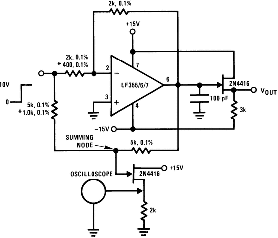
M38510/11402BGA 电路图
M38510/11402BGA 相关产品
- 5962-87738012A
- 5962-88513012A
- 5962-8851302HA
- 5962-8856501CA
- 5962-8859301M2A
- 5962-8872101PA
- 5962-8954401PA
- 5962-89641012A
- 5962-9098001MXA
- 5962-9201301MEA
- 5962-9313001MPA
- 5962-9452101M2A
- 5962-9457201MEA
- 5962-9457203MPA
- 5962-9851501QPA
- 77043012A
- 8102302PA
- 81023052A
- 81023062A
- 8102306CA
- ACPL-785E
- ACPL-785E-200
- AD524SD/883B
- AD524SE/883B
- AD549SH/883B
- AD603SQ/883B
- AD624SD/883B
- AD625SD/883B
- AD640TD/883B
- AD684SQ/883B