 搜索
搜索
 发布采购
发布采购
更新日期:2024-04-01 00:04:00

产品简介:适用于非色散红外 (NDIR) 传感应用的可配置 AFE
查看详情LMP91050MMX/NOPB 供应商
- 公司
- 型号
- 品牌
- 封装/批号
- 数量
- 地区
- 日期
- 说明
- 询价
-
TI
-
原厂原装
22+ -
3288
-
上海市
-
-
-
一级代理原装
-
TI(德州仪器)
-
VSSOP-10
2022+ -
12000
-
上海市
-
-
-
原装可开发票
LMP91050MMX/NOPB 中文资料属性参数
- 现有数量:0现货查看交期
- 价格:1 : ¥26.31000剪切带(CT)3,500 : ¥14.90607卷带(TR)
- 系列:-
- 包装:卷带(TR)剪切带(CT)Digi-Reel? 得捷定制卷带
- 产品状态:在售
- 位数:-
- 通道数:1
- 功率 (W):-
- 电压 - 供电,模拟:2.7V ~ 5.5V
- 电压 - 供电,数字:2.7V ~ 5.5V
- 安装类型:表面贴装型
- 封装/外壳:10-TFSOP,10-MSOP(0.118",3.00mm 宽)
- 供应商器件封装:10-VSSOP
产品特性
- Programmable Gain Amplifier
- Dark Signal Offset Cancellation
- Supports External Filtering
- Common-Mode Generator and 8-Bit DAC
- Key Specifications Programmable Gain 167 to 7986 V/V Low Noise (0.1 to 10 Hz) 0.1 µVRMS Gain Drift 100 ppm/°C (Maximum) Phase Delay Drift 500 ns (Maximum) Power Supply Voltage Range 2.7 to 5.5 V
- Programmable Gain 167 to 7986 V/V
- Low Noise (0.1 to 10 Hz) 0.1 µVRMS
- Gain Drift 100 ppm/°C (Maximum)
- Phase Delay Drift 500 ns (Maximum)
- Power Supply Voltage Range 2.7 to 5.5 V
产品概述
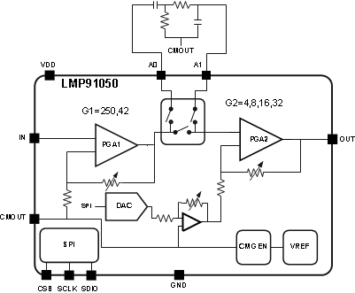
The LMP91050 device is a programmable integrated Sensor Analog Front End (AFE) optimized
for thermopile sensors, as typically used in NDIR applications. It provides a complete signal path
solution between a sensor and microcontroller that generates an output voltage proportional to the
thermopile voltage. The programmability of the LMP91050 enables it to support multiple thermopile
sensors with a single design as opposed to the multiple discrete solutions.The LMP91050 features a programmable gain amplifier (PGA), dark phase offset
cancellation, and an adjustable common-mode generator (1.15 V or 2.59 V)
which increases output dynamic range. The PGA offers a low-gain range
of 167 V/V to 1335 V/V plus a
high-gain range of 1002 V/V to 7986 V/V which enables the user to use
thermopiles with different
sensitivities. The PGA is highlighted by low-gain drift (100 ppm/°C),
output offset drift (1.2
mV/°C at G = 1002 V/V), phase delay drift (500 ns) and noise
specifications (0.1
µVRMS 0.1 to 10Hz).The offset cancellation circuitry compensates for the by adding an
equal and opposite offset to the input of the second stage, thus
removing the original offset from the output signal. This offset
cancellation circuitry allows
optimized usage of the ADC full scale and relaxes ADC resolution
requirements.The LMP91050 allows extra signal filtering (high-pass, lowpass or bandpass) through
dedicated pins A0 and A1, in order to remove out of band noise. The user can program through the on
board SPI interface. Available in a small form factor 10-pin package, the LMP91050 operates from
–40 to 105°C.
LMP91050MMX/NOPB 电路图
LMP91050MMX/NOPB 电路图
LMP91050MMX/NOPB 相关产品
- 5962-0720401VXC
- 5962-0720801VXC
- 5962-87802012A
- 5962-9152101MXA
- 5962-9961601HXA
- 6PA3100IRHBRQ1
- AD2S1210SST-EP-RL7
- AD2S1210WDSTZ
- AD2S80ATD/B
- AD3421QRWERQ1
- AD3421QRWETQ1
- AD5122ABCPZ100-RL7
- AD5122BCPZ100-RL7
- AD5122BRUZ10
- AD5123BCPZ100-RL7
- AD5142BCPZ10-RL7
- AD5235BRU25-EP-RL7
- AD5317RBRUZ
- AD5317RBRUZ-RL7
- AD5372BCPZ
- AD5623RBCPZ-5REEL7
- AD5628BCBZ-1-RL7
- AD5668BCPZ-1500RL7
- AD5684ARUZ
- AD5684BCPZ-RL7
- AD5684BRUZ-RL7
- AD5686ACPZ-RL7
- AD5686ARUZ
- AD5686BRUZ
- AD5686BRUZ-RL7