 搜索
搜索
 发布采购
发布采购
LMK04803BISQX/NOPB
时钟及计时器 IC(模拟)- 参考价格:¥67.48
更新日期:2024-04-01 00:04:00
LMK04803BISQX/NOPB 供应商
- 公司
- 型号
- 品牌
- 封装/批号
- 数量
- 地区
- 日期
- 说明
- 询价
-
TI
-
原厂原装
22+ -
3288
-
上海市
-
-
-
一级代理原装
-
TI(德州仪器)
-
WQFN-64(9x9)
2022+ -
12000
-
上海市
-
-
-
原装可开发票
LMK04803BISQX/NOPB 中文资料属性参数
- 制造商:National Semiconductor (TI)
- 输出端数量:12
- 输出电平:LVCMOS, LVPECL, LVDS
- 最大输出频率:3072
- Supply Voltage - Max:3.45 V
- Supply Voltage - Min:3.15 V
- 封装 / 箱体:WQFN-64
- 封装:Reel
- 最大工作温度:+ 85 C
- 最小工作温度:- 40 C
- 安装风格:SMD/SMT
- 工厂包装数量:2000
产品特性
- Ultra-Low RMS Jitter Performance 111 fs RMS Jitter (12 kHz to 20 MHz) 123 fs RMS Jitter (100 Hz to 20 MHz)
- 111 fs RMS Jitter (12 kHz to 20 MHz)
- 123 fs RMS Jitter (100 Hz to 20 MHz)
- Dual Loop PLLatinum™ PLL Architecture
- PLL1 Integrated Low-Noise Crystal Oscillator Circuit Holdover Mode when Input Clocks are Lost Automatic or Manual Triggering/Recovery
- Integrated Low-Noise Crystal Oscillator Circuit
- Holdover Mode when Input Clocks are Lost
- Automatic or Manual Triggering/Recovery
- PLL2 Normalized PLL Noise Floor of –227 dBc/Hz Phase Detector Rate up to 155 MHz OSCin Frequency-Doubler Integrated Low-Noise VCO
- Normalized PLL Noise Floor of –227 dBc/Hz
- Phase Detector Rate up to 155 MHz
- OSCin Frequency-Doubler
- Integrated Low-Noise VCO
- 2 Redundant Input Clocks with LOS Automatic and Manual Switch-Over Modes
- Automatic and Manual Switch-Over Modes
- 50 % Duty Cycle Output Divides, 1 to 1045 (Even and Odd)
- 12 LVPECL, LVDS, or LVCMOS Programmable Outputs
- Digital Delay: Fixed or Dynamically Adjustable
- 25 ps Step Analog Delay Control.
- 14 Differential Outputs. Up to 26 Single Ended. Up to 6 VCXO/Crystal Buffered Outputs
- Up to 6 VCXO/Crystal Buffered Outputs
- Clock Rates of up to 1536 MHz
- 0-Delay Mode
- Three Default Clock Outputs at Power Up
- Multi-Mode: Dual PLL, Single PLL, and Clock Distribution
- Industrial Temperature Range: –40 to 85°C
- 3.15-V to 3.45-V Operation
- 2 Dedicated Buffered/Divided OSCin Clocks
- Package: 64-Pin WQFN (9.0 × 9.0 × 0.8 mm)
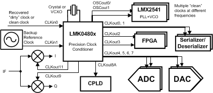
产品概述
The LMK0480x family is the industry’s highest performance clock conditioner with superior
clock jitter cleaning, generation, and distribution with advanced features to meet next generation
system requirements. The dual loop PLLatinum
architecture is capable of 111 fs rms jitter (12 kHz to 20 MHz) using a low noise VCXO module or
sub-200 fs rms jitter (12 kHz to 20 MHz) using a low cost external crystal and varactor
diode.The dual loop architecture consists of two high-performance phase-locked loops (PLL), a
low-noise crystal oscillator circuit, and a high-performance voltage controlled oscillator (VCO).
The first PLL (PLL1) provides low-noise jitter cleaner functionality while the second PLL (PLL2)
performs the clock generation. PLL1 can be configured to either work with an external VCXO module
or the integrated crystal oscillator with an external tunable crystal and varactor diode. When
paired with a very narrow loop bandwidth, PLL1 uses the superior close-in phase noise (offsets
below 50 kHz) of the VCXO module or the tunable crystal to clean the input clock. The output of
PLL1 is used as the clean input reference to PLL2 where it locks the integrated VCO. The loop
bandwidth of PLL2 can be optimized to clean the far-out phase noise (offsets above 50 kHz) where
the integrated VCO outperforms the VCXO module or tunable crystal used in PLL1.
LMK04803BISQX/NOPB 电路图
LMK04803BISQX/NOPB 电路图
LMK04803BISQX/NOPB 相关产品
- 100301QC
- 100304QC
- 100310QC
- 100311QC
- 100313QC
- 100316QC
- 100322QC
- 100329APC
- 100329DC
- 100336DC
- 100336PC
- 100341QC
- 100351DC
- 100351PC
- 100363QC
- 100364QC
- 100370QC
- 100390QC
- 100398QI
- 11AA010T-I/TT
- 11AA160T-I/TT
- 11LC010T-I/TT
- 11LC020T-I/TT
- 11LC040T-E/TT
- 11LC160T-E/TT
- 1ED020I12-F
- 2304NZGI-1LF
- 23A640-I/SN
- 23K256-I/SN
- 23K256-I/ST