 搜索
搜索
 发布采购
发布采购
LMK04033BISQE/NOPB
时钟及计时器 IC(模拟)- 参考价格:¥108.12-¥157.32
更新日期:2024-04-01 00:04:00
LMK04033BISQE/NOPB
时钟及计时器 IC(模拟)产品简介:具有 1840MHz 至 2160MHz VCO 的低噪声抖动消除器:2 路输出用于 2VPEC/LVPEC+LVDS+LVCMOS
查看详情- 参考价格:¥108.12-¥157.32
LMK04033BISQE/NOPB 供应商
- 公司
- 型号
- 品牌
- 封装/批号
- 数量
- 地区
- 日期
- 说明
- 询价
-
TI
-
原厂原装
22+ -
3288
-
上海市
-
-
-
一级代理原装
-
TI/德州仪器
-
QFN
21+ -
10000
-
杭州
-
-
-
只做原装现货,大量现货热卖
-
TI(德州仪器)
-
WQFN-48(7x7)
2022+ -
12000
-
上海市
-
-
-
原装可开发票
LMK04033BISQE/NOPB 中文资料属性参数
- 制造商:National Semiconductor (TI)
- 封装:Reel
- 最大工作温度:+ 85 C
- 最小工作温度:- 40 C
- 工厂包装数量:250
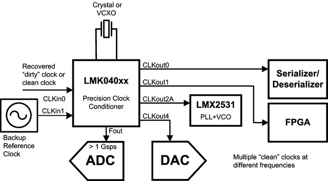
产品概述
The LMK04000 family of precision clock conditioners provides low-noise jitter cleaning, clock multiplication and distribution
without the need for high-performance voltage controlled crystal oscillators (VCXO) module. Using a cascaded PLLatinum architecture combined with an external crystal and varactor diode, the LMK04000 family provides sub-200 femtosecond (fs)
root mean square (RMS) jitter performance.
The cascaded architecture consists of two high-performance phase-locked loops (PLL), a low-noise crystal oscillator circuit,
and a high-performance voltage controlled oscillator (VCO). The first PLL (PLL1) provides a low-noise jitter cleaner function
while the second PLL (PLL2) performs the clock generation. PLL1 can be configured to either work with an external VCXO module
or use the integrated crystal oscillator with an external crystal and a varactor diode. When used with a very narrow loop
bandwidth, PLL1 uses the superior close-in phase noise (offsets below 50 kHz) of the VCXO module or the crystal to clean the
input clock. The output of PLL1 is used as the clean input reference to PLL2 where it locks the integrated VCO. The loop
bandwidth of PLL2 can be optimized to clean the far-out phase noise (offsets above 50 kHz) where the integrated VCO outperforms
the VCXO module or crystal used in PLL1.
The LMK04000 family features dual redundant inputs, five differential outputs, and an optional default-clock upon power up.
The input block is equipped with loss of signal detection and automatic or manual selection of the reference clock. Each
clock output consists of a programmable divider, a phase synchronization circuit, a programmable delay, and an LVDS, LVPECL,
or LVCMOS output buffer. The default startup clock is available on CLKout2 and it can be used to provide an initial clock
for the field-programmable gate array (FPGA) or microcontroller that programs the jitter cleaner during the system power up
sequence.
LMK04033BISQE/NOPB 数据手册
| 数据手册 | 说明 | 数量 | 操作 |
|---|---|---|---|
 LMK04033BISQE/NOPB LMK04033BISQE/NOPB
|
IC CLOCK CONDITIONER PREC 48WQFN |
65页,1.49M | 查看 |
LMK04033BISQE/NOPB 电路图
LMK04033BISQE/NOPB 电路图
LMK04033BISQE/NOPB 相关产品
- 100301QC
- 100304QC
- 100310QC
- 100311QC
- 100313QC
- 100316QC
- 100322QC
- 100329APC
- 100329DC
- 100336DC
- 100336PC
- 100341QC
- 100351DC
- 100351PC
- 100363QC
- 100364QC
- 100370QC
- 100390QC
- 100398QI
- 11AA010T-I/TT
- 11AA160T-I/TT
- 11LC010T-I/TT
- 11LC020T-I/TT
- 11LC040T-E/TT
- 11LC160T-E/TT
- 1ED020I12-F
- 2304NZGI-1LF
- 23A640-I/SN
- 23K256-I/SN
- 23K256-I/ST