 搜索
搜索
 发布采购
发布采购
LMH6502MT/NOPB
放大器 IC- 参考价格:¥26.63-¥43.68
更新日期:2024-04-01 00:04:00
LMH6502MT/NOPB 供应商
- 公司
- 型号
- 品牌
- 封装/批号
- 数量
- 地区
- 日期
- 说明
- 询价
-
TI
-
原厂原装
22+ -
3288
-
上海市
-
-
-
一级代理原装
-
TI
-
14-TSSOP
21+ -
10000
-
杭州
-
-
-
只做原装,大量现货供应
-
TI(德州仪器)
-
TSSOP-14
2022+ -
12000
-
上海市
-
-
-
原装可开发票
LMH6502MT/NOPB 中文资料属性参数
- 制造商:National Semiconductor (TI)
- 通道数量:1
- 共模抑制比(最小值):72 dB (Typ)
- 工作电源电压:9 V
- 电源电流:38 mA at +/- 5 V
- 最大工作温度:+ 85 C
- 最小工作温度:- 40 C
- 安装风格:SMD/SMT
- 封装 / 箱体:TSSOP-14
- 封装:Tube
- 双重电源电压:+/- 3 V, +/- 5 V
- 最大双重电源电压:+/- 6 V
- 最小双重电源电压:+/- 2.5 V
- 工厂包装数量:94
- Supply Voltage - Max:12 V
- Supply Voltage - Min:5 V
产品特性
- VS = ±5V, TA = 25°C, RF = 1kΩ, RG = 174Ω, RL = 100Ω, AV = AV(MAX) = 10 Typical Values Unless Specified.
- -3dB BW: 130MHz
- Gain Control BW: 100MHz
- Adjustment Range (Typical Over Temp): 70dB
- Gain Matching (Limit): ±0.6dB
- Slew Rate: 1800V/µs
- Supply Current (No Load): 27mA
- Linear Output Current: ±75mA
- Output Voltage (RL = 100Ω): ±3.2V
- Input Voltage Noise: 7.7nV/√Hz
- Input Current Noise: 2.4pA/√Hz
- THD (20MHz, RL = 100Ω, VO = 2VPP): −53dBc
- Replacement for CLC520
产品概述
The LMH6502 is a wideband DC coupled
differential input voltage controlled gain stage followed by a high-speed current feedback Op Amp
which can directly drive a low impedance load. Gain adjustment range is more than 70dB for up to
10MHz.Maximum gain is set by external components and the gain can be reduced all the way to
cut-off. Power consumption is 300mW with a speed of 130MHz. Output referred DC offset voltage is
less than 350mV over the entire gain control voltage range. Device-to-device Gain matching is
within ±0.6dB at maximum gain. Furthermore, gain at any VG is tested and the
tolerance is ensured. The output current feedback Op Amp allows high frequency large signals (Slew
Rate = 1800V/μs) and can also drive heavy load current (75mA). Differential inputs allow common
mode rejection in low level amplification or in applications where signals are carried over
relatively long wires. For single ended operation, the unused input can easily be tied to ground
(or to a virtual half-supply in single supply application). Inverting or non-inverting gains could
be obtained by choosing one input polarity or the other.To provide ease of use when working with a single supply, VG range
is set to be from 0V to +2V relative to pin 11 potential (ground pin). In single supply operation,
this ground pin is tied to a "virtual" half supply.LMH6502 gain control is linear in dB for a large portion of the total gain control range.
This makes the device suitable for AGC circuits among other applications. For linear gain control
applications, see the LMH6503 datasheet. The LMH6502 is available in the SOIC and TSSOP
package.
LMH6502MT/NOPB 数据手册
| 数据手册 | 说明 | 数量 | 操作 |
|---|---|---|---|
 LMH6502MT/NOPB LMH6502MT/NOPB
|
Variable Gain Amplifier 1 Circuit 14-TSSOP |
29页,1.57M | 查看 |
LMH6502MT/NOPB 电路图
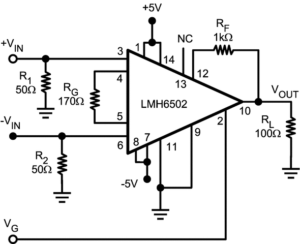
LMH6502MT/NOPB 电路图
LMH6502MT/NOPB 相关产品
- 100301QC
- 100304QC
- 100310QC
- 100311QC
- 100313QC
- 100316QC
- 100322QC
- 100329APC
- 100329DC
- 100336DC
- 100336PC
- 100341QC
- 100351DC
- 100351PC
- 100363QC
- 100364QC
- 100370QC
- 100390QC
- 100398QI
- 11AA010T-I/TT
- 11AA160T-I/TT
- 11LC010T-I/TT
- 11LC020T-I/TT
- 11LC040T-E/TT
- 11LC160T-E/TT
- 1ED020I12-F
- 2304NZGI-1LF
- 23A640-I/SN
- 23K256-I/SN
- 23K256-I/ST