 搜索
搜索
 发布采购
发布采购
- 参考价格:CNY 16.70-CNY 20.70
更新日期:2024-04-01 00:04:00
LMH2180SDE 供应商
- 公司
- 型号
- 品牌
- 封装/批号
- 数量
- 地区
- 日期
- 说明
- 询价
-
TI
-
原厂原装
22+ -
3288
-
上海市
-
-
-
一级代理原装
-
TI(德州仪器)
-
WSON-8(3x3)
2022+ -
12000
-
上海市
-
-
-
原装可开发票
-
NSC/ELNAF
-
QFN
1916+ -
190
-
上海市
-
-
-
原装现货,精专配套,正品BOM表报价
LMH2180SDE 中文资料属性参数
- 时钟类型::时钟缓冲器
- 频率::75MHz
- 输出通道数字::2
- 电源电流::2.3mA
- 电源电压范围::2.4V 到 5V
- 封装形式::LLP
- 针脚数::8
- 工作温度范围::-40°C 到 +85°C
- SVHC(高度关注物质)::No SVHC (19-Dec-2011)
- 器件标号::2180
- 封装类型::LLP 非回拉型
- 工作温度敏::-40°C
- 工作温度最高::85°C
- 时钟频率::75MHz
- 电压 Vcc 最低::2.4V
- 电压, Vcc 最大::5V
- 电源电压 最大::5V
- 电源电压 最小::2.4V
- 类型::Dual Clock Buffer
- 表面安装器件::表面安装
产品特性
- (Typical Values are: VSUPPLY = 2.7V and CL = 10 pF, unless Otherwise Specified.)
- Small Signal Bandwidth 78 MHz
- Supply Voltage Range 2.4V to 5V
- Phase Noise (VIN = 1 VPP, fC = 38.4 MHz, Δf = 1 kHz) −123 dBc/Hz
- Slew Rate 106 V/μs
- Total Supply Current 2.3 mA
- Shutdown Current 30 µA
- Rail-to-Rail Input and Output
- Individual Buffer Enable Pins
- Rapid Ton Technology
- Crosstalk Rejection Circuitry
- Packages:8-Pin WSON, Solder Bump and no Pullback 8-Bump DSBGA
- 8-Pin WSON, Solder Bump and no Pullback
- 8-Bump DSBGA
- Temperature Range −40°C to 85°C
产品概述
The LMH2180 is a high speed dual clock buffer designed for portable communications and
applications requiring multiple accurate multi-clock systems. The LMH2180 integrates two 75 MHz low
noise buffers with independent shutdown pins into a small package. The LMH2180 ensures superb
system operation between the baseband and the oscillator signal path by eliminating crosstalk
between the multiple clock signals.Unique technology and design provides the LMH2180 with the ability to accurately drive
both large capacitive and resistive loads. Low supply current combined with shutdown pins for each
channel means the LMH2180 is ideal for battery powered applications. This part does not use an
internal ground reference, thus providing additional system flexibility.The flexible buffers provide system designers the capacity to manage complex clock
signals in the latest wireless applications. Each buffer delivers 106 V/μs internal slew rate with
independent shutdown and duty cycle precision. Each input is internally biased to 1V, removing the
need for external resistors. Both channels have rail-to-rail inputs and outputs, a gain of one, and
are AC coupled with the use of one capacitor.Replacing a discrete buffer solution with the LMH2180 provides many benefits: simplified
board layout, minimized parasitic components, simplified BOM, design durability across multiple
applications, simplification of clock paths, and the ability to reduce the number of clock signal
generators in the system. The LMH2180 is produced in the tiny packages minimizing the required PCB
space.
LMH2180SDE 电路图
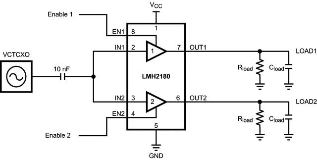
LMH2180SDE 电路图