 搜索
搜索
 发布采购
发布采购
- 参考价格:¥2.84-¥3.35
更新日期:2024-04-01 00:04:00

产品简介:单通道、36V、5MHz、高压摆率 (12V/μs)、输入接近 V+、JFET 输入运算放大器
查看详情- 参考价格:¥2.84-¥3.35
LF356N 供应商
- 公司
- 型号
- 品牌
- 封装/批号
- 数量
- 地区
- 日期
- 说明
- 询价
-
TI
-
原厂原装
22+ -
3288
-
上海市
-
-
-
一级代理原装
-
DIP-8P
0 -
50
-
杭州
-
-
-
原装正品现货
-
NS
-
-
2019+ -
5800
-
上海市
-
-
-
全新原装现货
-
NS
-
DIP8
22+授权代理 -
15800
-
上海市
-
-
-
旋尔只做进口原装,假一赔十...
-
TI(德州仪器)
-
DIP-8
2022+ -
12000
-
上海市
-
-
-
原装可开发票
-
NS
-
DIP-8
23+ -
15000
-
上海市
-
-
-
中国区代理原装现货热卖特价
-
TI/NS
-
DIP-8
21+ -
12000
-
上海市
-
-
-
原装现货,品质为先!请来电垂询!
-
NSC
-
DIP-8
新批号 -
887000
-
上海市
-
-
-
原厂发货进口原装微信同步QQ893727827
-
NS
-
DIP8
22+ -
3280
-
常州
-
-
-
原装现货假一罚十
-
NS
-
DIP8
23+ -
5800
-
上海市
-
-
-
进口原装现货,杜绝假货。
LF356N 中文资料属性参数
- 制造商:National Semiconductor (TI)
- 通道数量:1
- 共模抑制比(最小值):80 dB
- 输入补偿电压:10 mV at +/- 15 V
- 安装风格:Through Hole
- 封装 / 箱体:MDIP
- 转换速度:12 V/us at +/- 15 V
- 关闭:No
- 最大工作温度:+ 70 C
- 封装:Tube
- 最小工作温度:0 C
- 工厂包装数量:40
- 电源电流:10 mA at +/- 15 V
- 技术:BiFET
- 电压增益 dB:106.02 dB
产品特性
- Advantages Replace Expensive Hybrid and Module FET Op Amps Rugged JFETs Allow Blow-Out Free Handling Compared With MOSFET Input Devices Excellent for Low Noise Applications Using Either High or Low Source Impedance–Very Low 1/f Corner Offset Adjust Does Not Degrade Drift or Common-Mode Rejection as in Most Monolithic Amplifiers New Output Stage Allows Use of Large Capacitive Loads (5,000 pF) Without Stability Problems Internal Compensation and Large Differential Input Voltage Capability
- Replace Expensive Hybrid and Module FET Op Amps
- Rugged JFETs Allow Blow-Out Free Handling Compared With MOSFET Input Devices
- Excellent for Low Noise Applications Using Either High or Low Source Impedance–Very Low 1/f Corner
- Offset Adjust Does Not Degrade Drift or Common-Mode Rejection as in Most Monolithic Amplifiers
- New Output Stage Allows Use of Large Capacitive Loads (5,000 pF) Without Stability Problems
- Internal Compensation and Large Differential Input Voltage Capability
- Common Features Low Input Bias Current: 30 pA Low Input Offset Current: 3 pA High Input Impedance: 1012 Ω Low Input Noise Current: 0.01 pA/√Hz High Common-Mode Rejection Ratio: 100 dB Large DC Voltage Gain: 106 dB
- Low Input Bias Current: 30 pA
- Low Input Offset Current: 3 pA
- High Input Impedance: 1012 Ω
- Low Input Noise Current: 0.01 pA/√Hz
- High Common-Mode Rejection Ratio: 100 dB
- Large DC Voltage Gain: 106 dB
- Uncommon Features Extremely Fast Settling Time to 0.01%: 4 µs for the LFx55 devices 1.5 µs for the LFx56 1.5 µs for the LFx57 (AV = 5) Fast Slew Rate: 5 V/µs for the LFx55 12 V/µs for the LFx56 50 V/µs for the LFx57 (AV = 5) Wide Gain Bandwidth: 2.5 MHz for the LFx55 devices 5 MHz for the LFx56 20 MHz for the LFx57 (AV = 5) Low Input Noise Voltage: 20 nV/√Hz for the LFx55 12 nV/√Hz for the LFx56 12 nV/√Hz for the LFx57 (AV = 5)
- Extremely Fast Settling Time to 0.01%: 4 µs for the LFx55 devices 1.5 µs for the LFx56 1.5 µs for the LFx57 (AV = 5)
- 4 µs for the LFx55 devices
- 1.5 µs for the LFx56
- 1.5 µs for the LFx57 (AV = 5)
- Fast Slew Rate: 5 V/µs for the LFx55 12 V/µs for the LFx56 50 V/µs for the LFx57 (AV = 5)
- 5 V/µs for the LFx55
- 12 V/µs for the LFx56
- 50 V/µs for the LFx57 (AV = 5)
- Wide Gain Bandwidth: 2.5 MHz for the LFx55 devices 5 MHz for the LFx56 20 MHz for the LFx57 (AV = 5)
- 2.5 MHz for the LFx55 devices
- 5 MHz for the LFx56
- 20 MHz for the LFx57 (AV = 5)
- Low Input Noise Voltage: 20 nV/√Hz for the LFx55 12 nV/√Hz for the LFx56 12 nV/√Hz for the LFx57 (AV = 5)
- 20 nV/√Hz for the LFx55
- 12 nV/√Hz for the LFx56
- 12 nV/√Hz for the LFx57 (AV = 5)
产品概述
LF356N 数据手册
| 数据手册 | 说明 | 数量 | 操作 |
|---|---|---|---|
 LF356N LF356N
|
WIDE BANDWIDTH SINGLE J-FET OPERATIONAL AMPLIFIERS |
14 Pages页,1.05M | 查看 |
|
LF356N
|
Series Monolithic JFET Input Operational Amplifiers |
18 Pages页,1.05M | 查看 |
|
LF356N
|
JFET Input Operational Amplifiers |
23 Pages页,1.05M | 查看 |
|
LF356N/NOPB
|
IC, OP-AMP, 5MHZ, 12V/μs, DIP-8; Op Amp Type:General Purpose; No. of Amplifiers:1; Bandwidth:5MHz; Slew Rate:12V/μs; Supply Voltage Range:10V to 36V; Amplifier Case Style:DIP; No. of Pins:8; Operating Temperature Range:0°C to +70°C ;RoHS Compliant: Yes |
23页,1.05M | 查看 |
|
LF356N8
|
JFET-Input Operational Amplifiers Low Supply Current High Speed |
4 Pages页,423K | 查看 |
LF356N 电路图
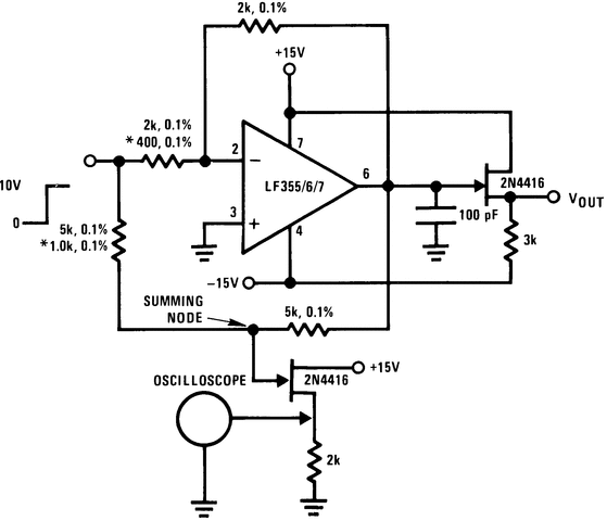
LF356N 电路图
LF356N 相关产品
- 100301QC
- 100304QC
- 100310QC
- 100311QC
- 100313QC
- 100316QC
- 100322QC
- 100329APC
- 100329DC
- 100336DC
- 100336PC
- 100341QC
- 100351DC
- 100351PC
- 100363QC
- 100364QC
- 100370QC
- 100390QC
- 100398QI
- 11AA010T-I/TT
- 11AA160T-I/TT
- 11LC010T-I/TT
- 11LC020T-I/TT
- 11LC040T-E/TT
- 11LC160T-E/TT
- 1ED020I12-F
- 2304NZGI-1LF
- 23A640-I/SN
- 23K256-I/SN
- 23K256-I/ST