 搜索
搜索
 发布采购
发布采购
更新日期:2024-04-01 00:04:00

产品简介:单片采样保持电路
查看详情JL198SGA 供应商
- 公司
- 型号
- 品牌
- 封装/批号
- 数量
- 地区
- 日期
- 说明
- 询价
-
National Semiconductor
-
TO-CAN-8
21+ -
50
-
上海市
-
-
-
一级代理原装
JL198SGA 中文资料属性参数
- 现有数量:0现货395Factory
- 价格:在售
- 系列:*
- 包装:托盘
- 产品状态:在售
- 放大器类型:-
- 电路数:-
- 输出类型:-
- 压摆率:-
- 增益带宽积:-
- -3db 带宽:-
- 电流 - 输入偏置:-
- 电压 - 输入补偿:-
- 电流 - 供电:-
- 电流 - 输出/通道:-
- 电压 - 跨度(最小值):-
- 电压 - 跨度(最大值):-
- 工作温度:-
- 安装类型:-
- 封装/外壳:-
- 供应商器件封装:-
产品特性
- Operates from ±5V to ±18V Supplies
- Less Than 10 μs Acquisition Time
- TTL, PMOS, CMOS Compatible Logic Input
- 0.5 mV Typical Hold Step at Ch = 0.01 μF
- Low Input Offset
- 0.002% Gain Accuracy
- Low Output Noise in Hold Mode
- Input Characteristics Do Not Change During Hold Mode
- High Supply Rejection Ratio in Sample or Hold
- Wide Bandwidth
- Space Qualified Logic Inputs on the LF198 are Fully Differential with Low Input Current, Allowing Direct Connection to TTL, PMOS, and CMOS. Differential Threshold is 1.4V. The LF198 will Operate from ±5V to ±18V Supplies.
产品概述
The LF198 is a monolithic sample-and-hold circuit which utilizes BI-FET technology to
obtain ultra-high dc accuracy with fast acquisition of signal and low droop rate. Operating as a
unity gain follower, dc gain accuracy is 0.002% typical and acquisition time is as low as 6 μs to
0.01%. A bipolar input stage is used to achieve low offset voltage and wide bandwidth. Input offset
adjust is accomplished with a single pin, and does not degrade input offset drift. The wide
bandwidth allows the LF198 to be included inside the feedback loop of 1 MHz op amps without having
stability problems. Input impedance of 1010Ω allows high source
impedances to be used without degrading accuracy.P-channel junction FET's are combined with bipolar devices in the output amplifier to
give droop rates as low as 5 mV/min with a 1 μF hold capacitor. The JFET's have much lower noise
than MOS devices used in previous designs and do not exhibit high temperature instabilities. The
overall design ensures no feed-through from input to output in the hold mode, even for input
signals equal to the supply voltages.
JL198SGA 电路图
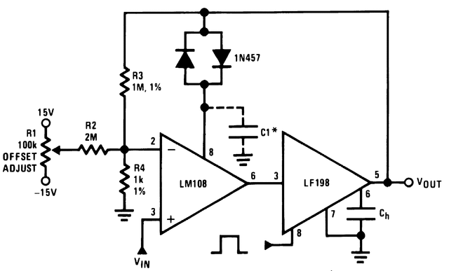
JL198SGA 电路图
JL198SGA 相关产品
- 5962-87738012A
- 5962-88513012A
- 5962-8851302HA
- 5962-8856501CA
- 5962-8859301M2A
- 5962-8872101PA
- 5962-8954401PA
- 5962-89641012A
- 5962-9098001MXA
- 5962-9201301MEA
- 5962-9313001MPA
- 5962-9452101M2A
- 5962-9457201MEA
- 5962-9457203MPA
- 5962-9851501QPA
- 77043012A
- 8102302PA
- 81023052A
- 81023062A
- 8102306CA
- ACPL-785E
- ACPL-785E-200
- AD524SD/883B
- AD524SE/883B
- AD549SH/883B
- AD603SQ/883B
- AD624SD/883B
- AD625SD/883B
- AD640TD/883B
- AD684SQ/883B