 搜索
搜索
 发布采购
发布采购
- 参考价格:¥143.52-¥187.82
更新日期:2024-04-01 00:04:00
JL156BGA 供应商
- 公司
- 型号
- 品牌
- 封装/批号
- 数量
- 地区
- 日期
- 说明
- 询价
-
National Semiconductor
-
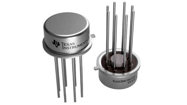
TO-CAN-8
21+ -
335
-
上海市
-
-
-
一级代理原装
JL156BGA 中文资料属性参数
- 制造商:National Semiconductor (TI)
- 通道数量:1
- 共模抑制比(最小值):85 dB
- 输入补偿电压:5 mV at +/- 5 V
- 安装风格:Through Hole
- 封装 / 箱体:TO-99
- 转换速度:7.5 V/us at +/- 15 V (Min)
- 关闭:No
- 最大工作温度:+ 125 C
- 最小工作温度:- 55 C
- 电源电流:7 mA at +/- 15 V
- 技术:BiFET
- 电压增益 dB:80 dB (Min)
产品特性
- AdvantagesReplace Expensive Hybrid and Module FET Op Amps Rugged JFETs Allow Blow-Out Free Handling Compared with MOSFET Input Devices Excellent for Low Noise Applications using either High or Low Source Impedance—Very Low 1/f Corner Offset Adjust does not Degrade Drift or Common-Mode Rejection as in Most Monolithic Amplifiers New Output Stage Allows use of Large Capacitive Loads (5,000 pF) without Stability Problems Internal Compensation and Large Differential Input Voltage Capability
- Replace Expensive Hybrid and Module FET Op Amps
- Rugged JFETs Allow Blow-Out Free Handling Compared with MOSFET Input Devices
- Excellent for Low Noise Applications using either High or Low Source Impedance—Very Low 1/f Corner
- Offset Adjust does not Degrade Drift or Common-Mode Rejection as in Most Monolithic Amplifiers
- New Output Stage Allows use of Large Capacitive Loads (5,000 pF) without Stability Problems
- Internal Compensation and Large Differential Input Voltage Capability
- Low Input Bias Current: 30pA
- Low Input Offset Current: 3pA
- High Input Impedance: 1012Ω
- Low Input Noise Current: 0.01 pA / √Hz
- High Common-Mode Rejection Ratio: 100 dB
- Large DC Voltage Gain: 106 dB
- Extremely Fast Settling Time to 0.01% 1.5μs
- Fast Slew Rate 12V/µs
- Wide Gain Bandwidth 5MHz
- Low Input Noise Voltage 12 nV / √Hz
产品概述
This is the first monolithic JFET input operational amplifier to incorporate well
matched, high voltage JFETs on the same chip with standard bipolar transistors (BI-FET™
Technology). This amplifier features low input bias and offset currents/low offset voltage and
offset voltage drift, coupled with offset adjust which does not degrade drift or common-mode
rejection. The device is also designed for high slew rate, wide bandwidth, extremely fast settling
time, low voltage and current noise and a low 1/ƒ noise corner.
JL156BGA 电路图
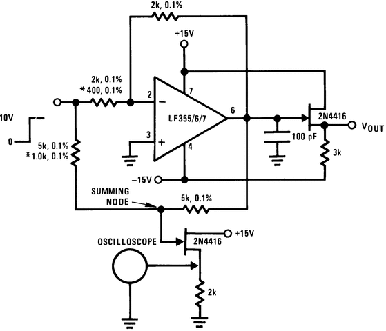
JL156BGA 电路图
JL156BGA 相关产品
- 100301QC
- 100304QC
- 100310QC
- 100311QC
- 100313QC
- 100316QC
- 100322QC
- 100329APC
- 100329DC
- 100336DC
- 100336PC
- 100341QC
- 100351DC
- 100351PC
- 100363QC
- 100364QC
- 100370QC
- 100390QC
- 100398QI
- 11AA010T-I/TT
- 11AA160T-I/TT
- 11LC010T-I/TT
- 11LC020T-I/TT
- 11LC040T-E/TT
- 11LC160T-E/TT
- 1ED020I12-F
- 2304NZGI-1LF
- 23A640-I/SN
- 23K256-I/SN
- 23K256-I/ST