 搜索
搜索
 发布采购
发布采购
更新日期:2024-04-01 00:04:00
产品简介:100MHz M-LVDS 线路驱动器/接收器组合
查看详情DS91C180TMA 供应商
- 公司
- 型号
- 品牌
- 封装/批号
- 数量
- 地区
- 日期
- 说明
- 询价
-
TI
-
原厂原装
22+ -
3288
-
上海市
-
-
-
一级代理原装
DS91C180TMA 中文资料属性参数
- 电源电压范围::3V 到 3.6V
- 封装形式::SOIC
- 针脚数::14
- 工作温度范围::-40°C 到 +85°C
- SVHC(高度关注物质)::No SVHC (19-Dec-2011)
- 器件标号::91
- 封装类型::SOIC
- 工作温度敏::-40°C
- 工作温度最高::85°C
- 接口类型::M-LVDS
- 接收器数::1
- 收发器类型::差分
- 数据率::200Mbps
- 电源电压 最大::3.6V
- 电源电压 最小::3V
- 电源电流::20mA
- 表面安装器件::表面安装
- 输出电流 最大::10μA
- 驱动器数::1
产品特性
- DC to 100+ MHz / 200+ Mbps Low Power, Low EMI Operation
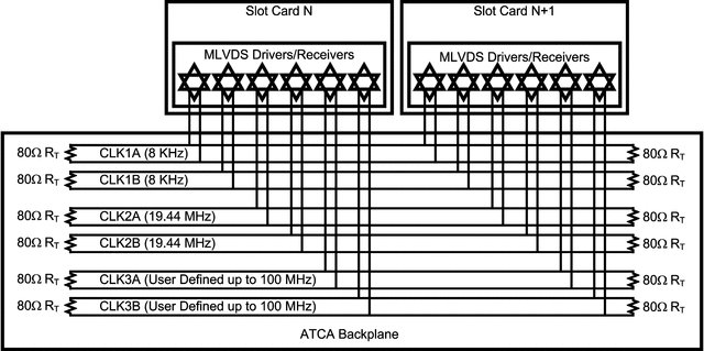
- Optimal for ATCA, uTCA Clock Distribution Networks
- Meets or Exceeds TIA/EIA-899 M-LVDS Standard
- Wide Input Common Mode Voltage for Increased Noise Immunity
- DS91D180 has Type 1 Receiver Input
- DS91C180 has Type 2 Receiver Input for Fail-Safe Functionality
- Industrial Temperature Range
- Space Saving SOIC-14 Package (JEDEC MS-012)
产品概述
The DS91D180 and DS91C180 are 100 MHz M-LVDS (Multipoint Low Voltage Differential
Signaling) line driver/receiver pairs designed for applications that utilize multipoint networks
(e.g. clock distribution in ATCA and uTCA based systems). M-LVDS is a bus interface standard
(TIA/EIA-899) optimized for multidrop networks. Controlled edge rates, tight input receiver
thresholds and increased drive strength are sone of the key enhancments that make M-LVDS devices an
ideal choice for distributing signals via multipoint networks.The DS91D180/DS91C180 driver input accepts LVTTL/LVCMOS signals and converts them to
differential M-LVDS signal levels. The DS91D180/DS91C180 receiver accepts low voltage differential
signals (LVDS, B-LVDS, M-LVDS, LV-PECL and CML) and converts them to 3V LVCMOS signals. The
DS91D180 device has a M-LVDS type 1 receiver input with no offset.The DS91C180 device has a type 2
receiver input which enable failsafe functionality.
DS91C180TMA 数据手册
| 数据手册 | 说明 | 数量 | 操作 |
|---|---|---|---|
 DS91C180TMA/NOPB DS91C180TMA/NOPB
|
1/1 Transceiver Full LVDS 14-SOICN |
18页,970K | 查看 |
DS91C180TMA 电路图
DS91C180TMA 电路图