 搜索
搜索
 发布采购
发布采购
- 参考价格:¥46.23-¥76.52
更新日期:2024-12-18 09:12:57
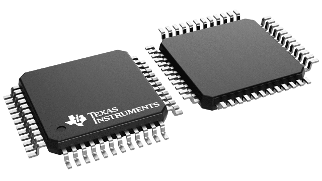
产品简介:5MHz 至 43MHz 直流平衡 24 位 FPD-Link II 串行器 - 汽车级
查看详情- 参考价格:¥46.23-¥76.52
DS90UR241QVS/NOPB 供应商
- 公司
- 型号
- 品牌
- 封装/批号
- 数量
- 地区
- 日期
- 说明
- 询价
-
DS90UR241QVS/NOPB
原装现货 -
TI
-
TQFP-48
22+ -
14
-
深圳
-
12-18
-
只做原装深圳现货
-
TI
-
原厂原装
22+ -
3288
-
上海市
-
-
-
一级代理原装
-
TI(德州仪器)
-
TQFP-48_7x7x05P
2022+ -
9
-
上海市
-
-
-
原装可开发票
DS90UR241QVS/NOPB 中文资料属性参数
- 制造商:National Semiconductor (TI)
- 激励器数量:1
- 接收机数量:24
- 工作电源电压:3.3 V
- 最大工作温度:+ 105 C
- 封装 / 箱体:TQFP-48
- 封装:Tray
- 最小工作温度:- 40 C
- 安装风格:SMD/SMT
- 工厂包装数量:250
- Supply Voltage - Max:3.6 V
- Supply Voltage - Min:3 V
- 类型:LVDS
产品特性
- Supports Displays With 18-Bit Color Depth
- 5-MHz to 43-MHz Pixel Clock
- Automotive-Grade Product AEC-Q100 Grade 2 Qualified
- 24:1 Interface Compression
- Embedded Clock With DC Balancing Supports AC-Coupled Data Transmission
- Capable to Drive up to 10 Meters Shielded Twisted-Pair Cable
- No Reference Clock Required (Deserializer)
- Meets ISO 10605 ESD – Greater than 8 kV HBM ESD Structure
- Hot Plug Support
- EMI Reduction – Serializer Accepts Spread Spectrum Input; Data Randomization and Shuffling on Serial Link; Deserializer Provides Adjustable PTO (Progressive Turnon) LVCMOS Outputs
- @Speed BIST (Built-In Self-Test) to Validate LVDS Transmission Path
- Individual Power-Down Controls for Both Transmitter and Receiver
- Power Supply Range 3.3 V ±10%
- 48-Pin TQFP Package for Transmitter and 64-Pin TQFP Package for Receiver
- Temperature Range: –40°C to 105°C
- Backward-Compatible Mode With DS90C241/DS90C124
产品概述
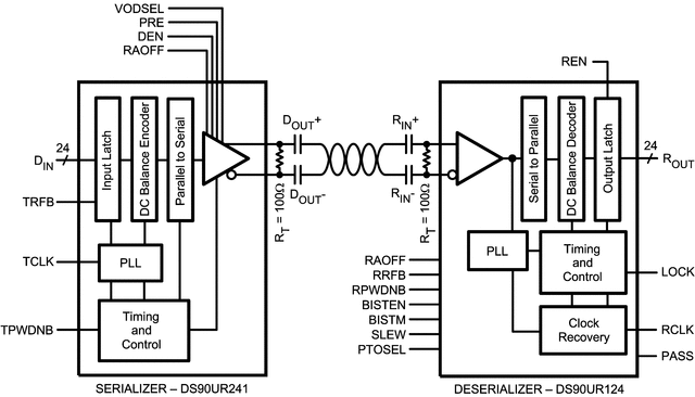
The DS90URxxx-Q1 chipset translates a 24-bit parallel bus into a fully transparent
data/control FPD-Link II LVDS serial stream with embedded clock information. This chipset is
ideally suited for driving graphical data to displays requiring 18-bit color depth: RGB666 + HS,
VS, DE + three additional general-purpose data channels. This single serial stream simplifies
transferring a 24-bit bus over PCB traces and cable by eliminating the skew problems between
parallel data and clock paths. The device saves system cost by narrowing data paths that in turn
reduce PCB layers, cable width, and connector size and pins.The DS90URxxx-Q1 incorporates FPD-Link II LVDS signaling on the high-speed I/O. FPD-Link
II LVDS provides a low-power and low-noise environment for reliably transferring data over a serial
transmission path. By optimizing the Serializer output edge rate for the operating frequency range,
EMI is further reduced.In addition, the device features pre-emphasis to boost signals over longer distances
using lossy cables. Internal DC-balanced encoding and decoding is used to support AC-coupled
interconnects. Using TI’s proprietary random lock, the parallel data of the Serializer are
randomized to the Deserializer without the need of REFCLK.
DS90UR241QVS/NOPB 电路图
DS90UR241QVS/NOPB 电路图
DS90UR241QVS/NOPB 相关产品
- 100301QC
- 100304QC
- 100310QC
- 100311QC
- 100313QC
- 100316QC
- 100322QC
- 100329APC
- 100329DC
- 100336DC
- 100336PC
- 100341QC
- 100351DC
- 100351PC
- 100363QC
- 100364QC
- 100370QC
- 100390QC
- 100398QI
- 11AA010T-I/TT
- 11AA160T-I/TT
- 11LC010T-I/TT
- 11LC020T-I/TT
- 11LC040T-E/TT
- 11LC160T-E/TT
- 1ED020I12-F
- 2304NZGI-1LF
- 23A640-I/SN
- 23K256-I/SN
- 23K256-I/ST