 搜索
搜索
 发布采购
发布采购
- 参考价格:¥24.01
更新日期:2024-04-01 00:04:00

产品简介:+3.3V LVDS 接收器 24 位平板显示 (FPD) 链接 - 85MHz
查看详情- 参考价格:¥24.01
DS90CF386SLCX 供应商
- 公司
- 型号
- 品牌
- 封装/批号
- 数量
- 地区
- 日期
- 说明
- 询价
-
TI
-
原厂原装
22+ -
3288
-
上海市
-
-
-
一级代理原装
-
TI(德州仪器)
-
NFBGA-64(8x8)
2022+ -
12000
-
上海市
-
-
-
原装可开发票
DS90CF386SLCX 中文资料属性参数
- 制造商:National Semiconductor (TI)
- 激励器数量:28
- 接收机数量:3
- 数据速率:2380 Mbps
- 工作电源电压:3.3 V
- 最大功率耗散:1610 mW
- 最大工作温度:+ 70 C
- 封装 / 箱体:FBGA
- 封装:Reel
- 最小工作温度:- 10 C
- 安装风格:SMD/SMT
- Supply Voltage - Max:3.6 V
- Supply Voltage - Min:3 V
- 类型:CMOS, TTL
产品特性
- 20-MHz to 85-MHz Shift Clock Support
- Rx Power Consumption <142 mW (Typical) at 85-MHz Grayscale
- Rx Power-Down Mode <1.44 mW (Maximum)
- ESD Rating >7 kV (HBM), >700 V (EIAJ)
- Supports VGA, SVGA, XGA, and Single Pixel SXGA
- PLL Requires No External Components
- Compatible With TIA/EIA-644 LVDS Standard
- Low Profile 56-Pin or 48-Pin TSSOP Package
- DS90CF386 Also Available in a 64-Pin, 0.8-mm, Fine Pitch Ball Grid Array (NFBGA) Package
产品概述
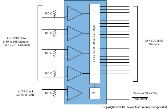
The DS90CF386 receiver converts four LVDS (Low Voltage Differential Signaling) data
streams back into parallel 28 bits of LVCMOS data. Also available is the DS90CF366 receiver that
converts three LVDS data streams back into parallel 21 bits of LVCMOS data. The outputs of both
receivers strobe on the falling edge. A rising edge or falling edge strobe transmitter will
interoperate with a falling edge strobe receiver without any translation logic.The receiver LVDS clock operates at rates from
20 MHz to 85 MHz. The device phase-locks to the input LVDS clock, samples the serial bit
streams at the LVDS data lines, and converts them into parallel output data. At an incoming clock
rate of 85 MHz, each LVDS input line is running at a bit rate of
595 Mbps, resulting in a maximum throughput of
2.38 Gbps for the DS90CF386 and 1.785 Gbps for the DS90CF366.The use of these serial link devices is ideal for solving EMI and cable size problems
associated with transmitting data over wide, high-speed parallel LVCMOS interfaces. Both devices
are offered in TSSOP packages. The DS90CF386 is also offered in a 64-pin, 0.8-mm, fine pitch ball
grid array (NFBGA) package which provides a 44% reduction in PCB footprint compared to the 56-pin
TSSOP package.
DS90CF386SLCX 电路图
DS90CF386SLCX 电路图
DS90CF386SLCX 相关产品
- 100301QC
- 100304QC
- 100310QC
- 100311QC
- 100313QC
- 100316QC
- 100322QC
- 100329APC
- 100329DC
- 100336DC
- 100336PC
- 100341QC
- 100351DC
- 100351PC
- 100363QC
- 100364QC
- 100370QC
- 100390QC
- 100398QI
- 11AA010T-I/TT
- 11AA160T-I/TT
- 11LC010T-I/TT
- 11LC020T-I/TT
- 11LC040T-E/TT
- 11LC160T-E/TT
- 1ED020I12-F
- 2304NZGI-1LF
- 23A640-I/SN
- 23K256-I/SN
- 23K256-I/ST