 搜索
搜索
 发布采购
发布采购
- 参考价格:CNY 44.40
更新日期:2024-04-01 00:04:00
产品简介:5MHz 至 35MHz 直流平衡 24 位汽车类 FPD-Link II 串行器
查看详情- 参考价格:CNY 44.40
DS90C241QVS 供应商
- 公司
- 型号
- 品牌
- 封装/批号
- 数量
- 地区
- 日期
- 说明
- 询价
-
NS
-
LQFP48
23+ -
5800
-
上海市
-
-
-
进口原装现货,杜绝假货。
-
NS/ELNAF
-
TQFP
1902+ -
500
-
上海市
-
-
-
原装现货,精专配套,正品BOM表报价
-
TI
-
TSSOP
23+ -
46000
-
合肥
-
-
-
科大讯飞战略投资企业,提供一站式配套服务
-
TI
-
原厂原装
22+ -
3288
-
上海市
-
-
-
一级代理原装
-
TI(德州仪器)
-
TQFP-48(7x7)
2022+ -
12000
-
上海市
-
-
-
原装可开发票
DS90C241QVS 中文资料属性参数
- 电源电压范围::3V 到 3.6V
- 封装形式::TQFP
- 针脚数::48
- 工作温度范围::-40°C 到 +105°C
- MSL::MSL 3 - 168小时
- SVHC(高度关注物质)::No SVHC (19-Dec-2011)
- 器件标号::90
- 封装类型::TQFP
- 工作温度敏::-40°C
- 工作温度最高::105°C
- 接口::LVDS
- 接口类型::LVDS
- 收发器类型::低压差分(LVDS)
- 电源电压 最大::3.6V
- 电源电压 最小::3V
- 线/总线驱动器/接收器/收发器 类型::LVDS Serializer
- 表面安装器件::表面安装
- 驱动器数::1
产品特性
- 5-MHz to 35-MHz Clock Embedded and DC-Balancing 24:1 and 1:24 Data Transmissions
- User Defined Pre-Emphasis Driving Ability Through External Resistor on LVDS Outputs and Capable to Drive Up to 10-Meter Shielded Twisted-Pair Cable
- User-Selectable Clock Edge for Parallel Data on Both Transmitter and Receiver
- Internal DC Balancing Encode and Decode (Supports AC-Coupling Interface With No External Coding Required)
- Individual Power-Down Controls for Both Transmitter and Receiver
- Embedded Clock CDR (Clock and Data Recovery) on Receiver and No External Source of Reference Clock Required
- All Codes RDL (Random Data Lock) to Support Live-Pluggable Applications
- LOCK Output Flag to Ensure Data Integrity at Receiver Side
- Balanced TSETUP and THOLD Between RCLK and RDATA on Receiver Side
- PTO (Progressive Turnon) LVCMOS Outputs to Reduce EMI and Minimize SSO Effects
- All LVCMOS Inputs and Control Pins Have Internal Pulldown
- On-Chip Filters for PLLs on Transmitter and Receiver
- Temperature Range: –40°C to 105°C
- Greater Than 8-kV HBM ESD Tolerant
- Meets AEC-Q100 Compliance
- Power Supply Range: 3.3 V ± 10%
- 48-Pin TQFP Package
产品概述
The DS90C241 and DS90C124 chipset translates a 24-bit parallel bus into a fully
transparent data and control LVDS serial stream with embedded clock information. This single serial
stream simplifies transferring a 24-bit bus over PCB traces or over cable by eliminating the skew
problems between parallel data and clock paths. It saves system cost by narrowing data paths, which
in turn reduces PCB layers, cable width, and connector size and pins.The DS90C241 and DS90C124 incorporate LVDS signaling on the high-speed I/O. LVDS provides
a low-power and low-noise environment for reliably transferring data over a serial transmission
path. By optimizing the serializer output edge rate for the operating frequency range, EMI is
further reduced.In addition, the device features pre-emphasis to boost signals over longer distances
using lossy cables. Internal DC balanced encoding and decoding supports AC-coupled
interconnects.
DS90C241QVS 数据手册
| 数据手册 | 说明 | 数量 | 操作 |
|---|---|---|---|
 DS90C241QVS/NOPB DS90C241QVS/NOPB
|
840Mbps Serializer 24 Input 1 Output 48-TQFP (7x7) |
31页,987K | 查看 |
DS90C241QVS 电路图
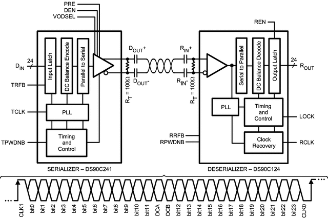
DS90C241QVS 电路图