 搜索
搜索
 发布采购
发布采购
- 参考价格:¥48.51-¥85.28
更新日期:2024-04-01 00:04:00
产品简介:具有发送预加重和接收均衡功能的双路 4.0Gbps 2:1/1:2 CML 多路复用器/缓冲器
查看详情- 参考价格:¥48.51-¥85.28
DS40MB200SQ/NOPB 供应商
- 公司
- 型号
- 品牌
- 封装/批号
- 数量
- 地区
- 日期
- 说明
- 询价
-
TI
-
原厂原装
22+ -
3288
-
上海市
-
-
-
一级代理原装
-
TI/德州仪器
-
WQFN48
21+ -
10000
-
杭州
-
-
-
只做原装现货,大量现货热卖
-
TI(德州仪器)
-
WQFN-48
2022+ -
12000
-
上海市
-
-
-
原装可开发票
-
TI
-
TSSOP
23+ -
46000
-
合肥
-
-
-
科大讯飞战略投资企业,提供一站式配套服务
DS40MB200SQ/NOPB 中文资料属性参数
- 制造商:National Semiconductor (TI)
- 输入线路数量:12
- 输出线路数量:12
- 极性:Non-Inverting
- Supply Voltage - Max:3.465 V
- Supply Voltage - Min:3.135 V
- 最大工作温度:+ 85 C
- 安装风格:SMD/SMT
- 封装 / 箱体:LLP-48
- 封装:Reel
- 数据速率:4 Gbps
- 最小工作温度:- 40 C
- 工厂包装数量:250
产品特性
- 1-Gbps to 4-Gbps Low Jitter Operation
- Fixed Input Equalization
- Programmable Output Pre-Emphasis
- Independent Switch and Line Side Pre-Emphasis Controls
- Programmable Switch-Side Loopback Mode
- On-Chip Terminations
- 3.3-V Supply
- ESD Rating of 6-kV HBM
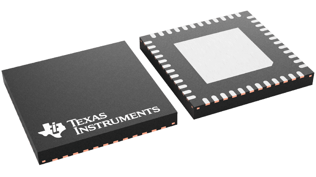
- 48-leadless WQFN Package (7 mm × 7 mm)
- 0°C to +85°C Operating Temperature Range
产品概述
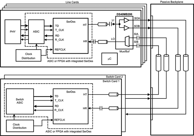
The DS40MB200 device is a dual signal conditioning 2:1 multiplexer (MUX) and 1:2 fan-out buffer designed for use in backplane-redundancy applications. Signal conditioning features include continuous time linear equalization (CTLE) and programmable output pre-emphasis, extending data communication in FR4 backplanes at rates up to 4 Gbps. Each input stage has a fixed equalizer to reduce intersymbol interference distortion from board traces.All output drivers have four selectable steps of pre-emphasis to compensate for transmission losses from long FR4 backplanes and reduce deterministic jitter. The pre-emphasis levels can be independently controlled for the line-side and switch-side drivers. The internal loopback paths from switch-side input to switch-side output enable at-speed system testing. All receiver inputs are internally terminated with 100-Ω differential terminating resistors. All drivers are internally terminated with 50 Ω to VCC.
DS40MB200SQ/NOPB 电路图
DS40MB200SQ/NOPB 电路图
DS40MB200SQ/NOPB 相关产品
- 100301QC
- 100304QC
- 100310QC
- 100311QC
- 100313QC
- 100316QC
- 100322QC
- 100329APC
- 100329DC
- 100336DC
- 100336PC
- 100341QC
- 100351DC
- 100351PC
- 100363QC
- 100364QC
- 100370QC
- 100390QC
- 100398QI
- 11AA010T-I/TT
- 11AA160T-I/TT
- 11LC010T-I/TT
- 11LC020T-I/TT
- 11LC040T-E/TT
- 11LC160T-E/TT
- 1ED020I12-F
- 2304NZGI-1LF
- 23A640-I/SN
- 23K256-I/SN
- 23K256-I/ST