 搜索
搜索
 发布采购
发布采购
- 封装:8-TSSOP,8-MSOP(0.118",3.00mm 宽)
- RoHS:无铅 / 符合限制有害物质指令(RoHS)规范要求
- 包装方式:带卷 (TR)
- 参考价格:$3.6
更新日期:2024-04-01 00:04:00
产品简介:16 位、双通道、超低短时脉冲波形干扰、电压输出数模转换器
查看详情- 封装:8-TSSOP,8-MSOP(0.118",3.00mm 宽)
- RoHS:无铅 / 符合限制有害物质指令(RoHS)规范要求
- 包装方式:带卷 (TR)
- 参考价格:$3.6
DAC8552IDGKR 供应商
- 公司
- 型号
- 品牌
- 封装/批号
- 数量
- 地区
- 日期
- 说明
- 询价
-
TI
-
原厂原装
22+ -
3288
-
上海市
-
-
-
一级代理原装
-
TI/德州仪器
-
7500
21+ -
10000
-
杭州
-
-
-
只做原装现货,大量现货热卖
-
TI(德州仪器)
-
VSSOP-8
2022+ -
12000
-
上海市
-
-
-
原装可开发票
-
TI/BB
-
MSOP-8
23+ -
15000
-
上海市
-
-
-
中国区代理原装现货热卖特价
-
TI
-
MSOP8
新批号 -
8877000
-
上海市
-
-
-
原厂发货进口原装微信同步QQ893727827
-
TI
-
MSOP8
23+ -
5800
-
上海市
-
-
-
进口原装现货,杜绝假货。
DAC8552IDGKR 中文资料属性参数
- 产品培训模块:Data Converter Basics
- 标准包装:2,500
- 类别:集成电路 (IC)
- 家庭:数据采集 - 数模转换器
- 系列:-
- 设置时间:8µs
- 位数:16
- 数据接口:串行
- 转换器数目:2
- 电压电源:单电源
- 功率耗散(最大):3mW
- 工作温度:-40°C ~ 105°C
- 安装类型:表面贴装
- 封装/外壳:8-TSSOP,8-MSOP(0.118",3.00mm 宽)
- 供应商设备封装:8-MSOP
- 包装:带卷 (TR)
- 输出数目和类型:2 电压,单极;2 电压,双极
- 采样率(每秒):200k
- 配用:296-30876-ND - EVAL MODULE FOR DAC8552
产品特性
- Relative Accuracy: 4LSB
- Glitch Energy: 0.15nV-s
- MicroPower Operation: 155µA per Channel at 2.7V
- Power-On Reset to Zero-Scale
- Power Supply: 2.7V to 5.5V
- 16-Bit Monotonic Over Temperature
- Settling Time: 10µs to ±0.003% FSR
- Ultra-Low AC Crosstalk: -100dB Typ
- Low-Power Serial Interface with Schmitt-Triggered Inputs
- On-Chip Output Buffer Amplifier with Rail-to-Rail Operation
- Double-Buffered Input Architecture
- Simultaneous or Sequential Output Update and Power-down
- Available in a Tiny MSOP-8 Package
- APPLICATIONSPortable InstrumentationClosed-Loop Servo ControlProcess ControlData Acquisition SystemsProgrammable AttenuationPC Peripherals
- Portable Instrumentation
- Closed-Loop Servo Control
- Process Control
- Data Acquisition Systems
- Programmable Attenuation
- PC Peripherals
产品概述
The DAC8552 is a 16-bit, dual channel, voltage output digital-to-analog converter (DAC) offering low power operation and a flexible serial host interface. Each on-chip precision output amplifier allows rail-to-rail output swing to be achieved over the supply range of 2.7V to 5.5V. The device supports a standard 3-wire serial interface capable of operating with input data clock frequencies up to 30MHz for VDD = 5V.The DAC8552 requires an external reference voltage to set the output range of each DAC channel. Also incorporated into the device is a power-on reset circuit which ensures that the DAC outputs power up at zero-scale and remain there until a valid write takes place. The DAC8552 provides a flexible power-down feature, accessed over the serial interface, that reduces the current consumption of the device to 700nA at 5V.The low-power consumption of this device in normal operation makes it ideally suited for portable, battery-operated equipment and other low-power applications. The power consumption is 0.5mW per channel at 2.7V, reducing to 1µW in power-down mode.The DAC8552 is available in a MSOP-8 package with a specified operating temperature range of -40°C to +105°C.
DAC8552IDGKR 电路图
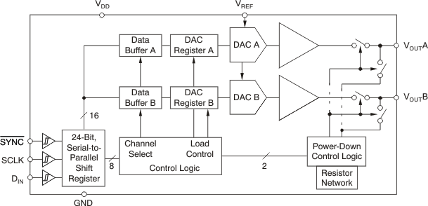
DAC8552IDGKR 电路图
DAC8552IDGKR 相关产品
- AD1833AASTZ
- AD1851RZ-J
- AD1851RZ-REEL7
- AD1852JRSZRL
- AD1856RZ
- AD1859JRZ-RL
- AD1866RZ-REEL
- AD1933WBSTZ
- AD1934WBSTZ
- AD1953YSTZ
- AD1954YSTZ
- AD1954YSTZRL
- AD1955ARSZ
- AD1955ARSZRL
- AD420AR-32-REEL
- AD420ARZ-32
- AD420ARZ-32-REEL
- AD421BR
- AD421BRZ
- AD421BRZRL
- AD421BRZRL7
- AD5024BRUZ
- AD5024BRUZ-REEL7
- AD5025BRUZ
- AD5040BRJZ-REEL7
- AD5044BRUZ
- AD5060ARJZ-2REEL7
- AD5060BRJZ-1500RL7
- AD5060BRJZ-1REEL7
- AD5060BRJZ-2500RL7