 搜索
搜索
 发布采购
发布采购
- 封装:8-TSSOP,8-MSOP(0.118",3.00mm 宽)
- RoHS:无铅 / 符合限制有害物质指令(RoHS)规范要求
- 包装方式:Digi-Reel®
- 参考价格:$5.4435-$7.35
更新日期:2024-04-01 00:04:00
产品简介:16 位、超低短时脉冲波形干扰、电压输出数模转换器
查看详情- 封装:8-TSSOP,8-MSOP(0.118",3.00mm 宽)
- RoHS:无铅 / 符合限制有害物质指令(RoHS)规范要求
- 包装方式:Digi-Reel®
- 参考价格:$5.4435-$7.35
DAC8551IDGKT 供应商
- 公司
- 型号
- 品牌
- 封装/批号
- 数量
- 地区
- 日期
- 说明
- 询价
-
TI
-
原厂原装
22+ -
3288
-
上海市
-
-
-
一级代理原装
-
TI
-
-
2019+ -
3000
-
上海市
-
-
-
全新原装现货
-
TI(德州仪器)
-
VSSOP-8
2022+ -
12000
-
上海市
-
-
-
原装可开发票
-
TI
-
MSOP-8
23+ -
15000
-
上海市
-
-
-
中国区代理原装现货热卖特价
-
TI代理
-
MSOP-8
新批号 -
7899
-
上海市
-
-
-
原厂发货进口原装微信同步QQ893727827
-
TI
-
8MSOP
23+ -
5800
-
上海市
-
-
-
进口原装现货,杜绝假货。
DAC8551IDGKT 中文资料属性参数
- 产品培训模块:Data Converter Basics
- 标准包装:1
- 类别:集成电路 (IC)
- 家庭:数据采集 - 数模转换器
- 系列:-
- 设置时间:8µs
- 位数:16
- 数据接口:串行,SPI?
- 转换器数目:1
- 电压电源:单电源
- 功率耗散(最大):1mW
- 工作温度:-40°C ~ 105°C
- 安装类型:表面贴装
- 封装/外壳:8-TSSOP,8-MSOP(0.118",3.00mm 宽)
- 供应商设备封装:8-MSOP
- 包装:®
- 输出数目和类型:1 电压,单极;1 电压,双极
- 采样率(每秒):200k
- 配用:296-20838-ND - EVALUATION MODULE FOR DAC8551
- 其它名称:296-18290-6
产品特性
- Relative Accuracy: 8LSB
- Glitch Energy: 0.1 nV-s
- MicroPower Operation: 140 µA at 2.7 V
- Power-On Reset to Zero
- Power Supply: 2.7 V to 5.5 V
- 16-Bit Monotonic
- Settling Time: 10 µs to ±0.003% FSR
- Low-Power Serial Interface with Schmitt-Triggered Inputs
- On-Chip Output Buffer Amplifier with Rail-to-Rail Operation
- Power-Down Capability
- Binary Input
- SYNC Interrupt Facility
- Drop-In Compatible With DAC85x1 and DAC8550 (2’s Complement Input)
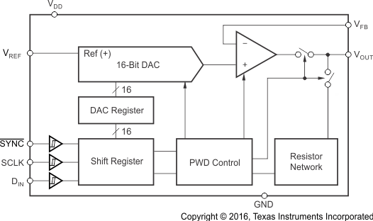
产品概述
The DAC8551 is a small, low-power, voltage output, 16-bit digital-to-analog converter
(DAC). It is monotonic, provides good linearity, and minimizes undesired code-to-code transient
voltages. The DAC8551 uses a versatile 3-wire serial interface that operates at clock rates to 30
MHz and is compatible with standard SPI™,
QSPI™, Microwire™, and digital signal processor (DSP)
interfaces.The DAC8551 requires an external reference voltage to set its output range. The DAC8551
incorporates a power-on-reset circuit that ensures the DAC output powers up at 0 V and remains
there until a valid write takes place to the device. The DAC8551 contains a power-down feature,
accessed over the serial interface, that reduces the current consumption of the device to 200 nA at
5 V.The low-power consumption of this device in normal operation makes it ideally suited for
portable, battery-operated equipment. The power consumption is 0.38 mW at 2.7 V,
reducing to less than 1 µW in power‑down
mode.For additional flexibilty, see the DAC8550 (SLAS476), a 2’s complement-input counterpart to the DAC8551.
DAC8551IDGKT 数据手册
| 数据手册 | 说明 | 数量 | 操作 |
|---|---|---|---|
 DAC8551IDGKT DAC8551IDGKT
|
16-BIT, ULTRA-LOW GLITCH, VOLTAGE OUTPUT DIGITAL-TO-ANALOG CONVERTER |
22 Pages页,1.7M | 查看 |
DAC8551IDGKT 电路图
DAC8551IDGKT 电路图
DAC8551IDGKT 相关产品
- AD1833AASTZ
- AD1851RZ-J
- AD1851RZ-REEL7
- AD1852JRSZRL
- AD1856RZ
- AD1859JRZ-RL
- AD1866RZ-REEL
- AD1933WBSTZ
- AD1934WBSTZ
- AD1953YSTZ
- AD1954YSTZ
- AD1954YSTZRL
- AD1955ARSZ
- AD1955ARSZRL
- AD420AR-32-REEL
- AD420ARZ-32
- AD420ARZ-32-REEL
- AD421BR
- AD421BRZ
- AD421BRZRL
- AD421BRZRL7
- AD5024BRUZ
- AD5024BRUZ-REEL7
- AD5025BRUZ
- AD5040BRJZ-REEL7
- AD5044BRUZ
- AD5060ARJZ-2REEL7
- AD5060BRJZ-1500RL7
- AD5060BRJZ-1REEL7
- AD5060BRJZ-2500RL7