 搜索
搜索
 发布采购
发布采购
- 封装:6-TSSOP,SC-88,SOT-363
- RoHS:无铅 / 符合限制有害物质指令(RoHS)规范要求
- 包装方式:Digi-Reel®
- 参考价格:$3.645-$6.97
更新日期:2024-04-01 00:04:00
产品简介:采用 SC70 封装的 16 位、单通道、80uA、2.0V-5.5V DAC
查看详情- 封装:6-TSSOP,SC-88,SOT-363
- RoHS:无铅 / 符合限制有害物质指令(RoHS)规范要求
- 包装方式:Digi-Reel®
- 参考价格:$3.645-$6.97
DAC8411IDCKT 供应商
- 公司
- 型号
- 品牌
- 封装/批号
- 数量
- 地区
- 日期
- 说明
- 询价
-
TI
-
原厂原装
22+ -
3288
-
上海市
-
-
-
一级代理原装
-
TI(德州仪器)
-
SC-70-6(SOT-363)
2022+ -
12000
-
上海市
-
-
-
原装可开发票
-
BB
-
SMD
22+ -
5000
-
常州
-
-
-
全新原装现货热卖
DAC8411IDCKT 中文资料属性参数
- 产品培训模块:Data Converter Basics
- 标准包装:1
- 类别:集成电路 (IC)
- 家庭:数据采集 - 数模转换器
- 系列:-
- 设置时间:6µs
- 位数:16
- 数据接口:串行
- 转换器数目:1
- 电压电源:单电源
- 功率耗散(最大):880µW
- 工作温度:-40°C ~ 125°C
- 安装类型:表面贴装
- 封装/外壳:6-TSSOP,SC-88,SOT-363
- 供应商设备封装:SC-70-6
- 包装:®
- 输出数目和类型:1 电压,单极;1 电压,双极
- 采样率(每秒):*
- 其它名称:296-23761-6
产品特性
- Relative Accuracy: 1 LSB INL (DAC8311: 14-bit) 4 LSB INL (DAC8411: 16-bit)
- 1 LSB INL (DAC8311: 14-bit)
- 4 LSB INL (DAC8411: 16-bit)
- Power Operation: 80 µA at 2 V
- Power-Down: 0.5 µA at 5 V, 0.1 µA at 2 V
- Wide Power Supply: 2 V to 5.5 V
- Power-On Reset to Zero Scale
- Straight Binary Data Format
- Low Power Serial Interface With Schmitt- Triggered Inputs: Up to 50 MHz
- On-Chip Output Buffer Amplifier, Rail-to- Rail Operation
- SYNC Interrupt Facility
- Extended Temperature Range –40°C to 125°C
- Pin-Compatible Family in a Tiny, 6-Pin SC70 Package
产品概述
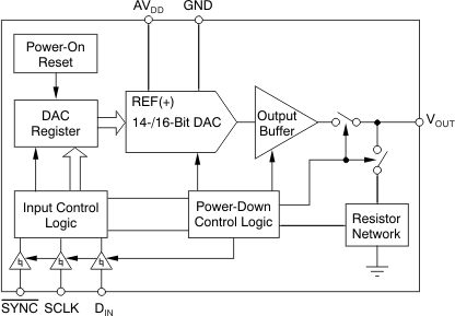
The DAC8311 (14-bit) and DAC8411 (16-bit) devices are low-power, single-channel, voltage
output digital-to-analog converters (DAC). They provide excellent linearity and minimize undesired
code-to-code transient voltages while offering an easy upgrade path within a pin-compatible family.
All devices use a versatile, 3-wire serial interface that operates at clock rates of up to 50 MHz
and is compatible with standard SPI,
QSPI, Microwire, and digital signal processor (DSP)
interfaces.All devices use an external power supply as a reference voltage to set the output range.
The devices incorporate a power-on reset (POR) circuit that ensures the DAC output powers up at 0 V
and remains there until a valid write to the device occurs. The DAC8311 and DAC8411 contain a
power-down feature, accessed over the serial interface, that reduces current consumption of the
device to 0.1 µA at 2 V in power down mode. The low power consumption of these devices in normal
operation makes it ideally suited for portable, battery-operated equipment. The power consumption
is 0.55 mW at 5 V, reducing to 2.5 µW in power-down mode.These devices are pin-compatible with the
DAC5311,
DAC6311,
and DAC7311, offering an easy
upgrade path from 8-, 10-, and 12-bit resolution to 14- and 16-bit. All devices are available in a
small, 6-pin, SC70 package. This package offers a flexible, pin-compatible, and
functionally-compatible drop-in solution within the family over an extended temperature range of
–40°C to 125°C.
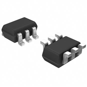
DAC8411IDCKT 电路图
DAC8411IDCKT 电路图
DAC8411IDCKT 相关产品
- AD1833AASTZ
- AD1851RZ-J
- AD1851RZ-REEL7
- AD1852JRSZRL
- AD1856RZ
- AD1859JRZ-RL
- AD1866RZ-REEL
- AD1933WBSTZ
- AD1934WBSTZ
- AD1953YSTZ
- AD1954YSTZ
- AD1954YSTZRL
- AD1955ARSZ
- AD1955ARSZRL
- AD420AR-32-REEL
- AD420ARZ-32
- AD420ARZ-32-REEL
- AD421BR
- AD421BRZ
- AD421BRZRL
- AD421BRZRL7
- AD5024BRUZ
- AD5024BRUZ-REEL7
- AD5025BRUZ
- AD5040BRJZ-REEL7
- AD5044BRUZ
- AD5060ARJZ-2REEL7
- AD5060BRJZ-1500RL7
- AD5060BRJZ-1REEL7
- AD5060BRJZ-2500RL7