 搜索
搜索
 发布采购
发布采购
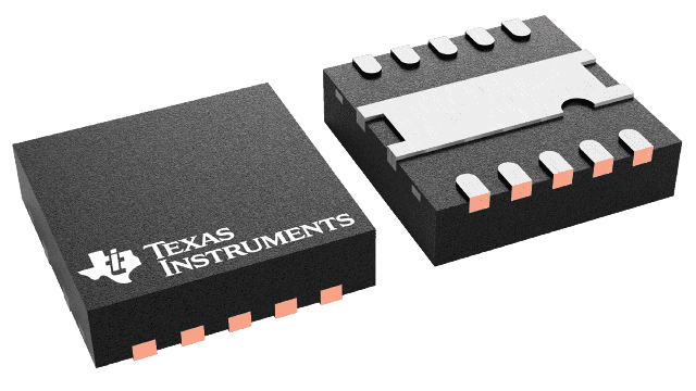
- 封装:10-WFDFN 裸露焊盘
- RoHS:无铅 / 符合限制有害物质指令(RoHS)规范要求
- 包装方式:Digi-Reel®
- 参考价格:$4.41788-$8.94
更新日期:2024-04-01 00:04:00
产品简介:具有 2.5V、4ppm/°C 基准的 14 位、双通道、低功耗、超低短时脉冲波形干扰、缓冲电压输出 DAC
查看详情- 封装:10-WFDFN 裸露焊盘
- RoHS:无铅 / 符合限制有害物质指令(RoHS)规范要求
- 包装方式:Digi-Reel®
- 参考价格:$4.41788-$8.94
DAC8163SDSCR 供应商
- 公司
- 型号
- 品牌
- 封装/批号
- 数量
- 地区
- 日期
- 说明
- 询价
-
TI
-
原厂原装
22+ -
3288
-
上海市
-
-
-
一级代理原装
DAC8163SDSCR 中文资料属性参数
- 标准包装:1
- 类别:集成电路 (IC)
- 家庭:数据采集 - 数模转换器
- 系列:-
- 设置时间:10µs
- 位数:14
- 数据接口:DSP,MICROWIRE?,QSPI?,串行,SPI?
- 转换器数目:2
- 电压电源:单电源
- 功率耗散(最大):7.15mW
- 工作温度:-40°C ~ 125°C
- 安装类型:表面贴装
- 封装/外壳:10-WFDFN 裸露焊盘
- 供应商设备封装:10-SON 裸露焊盘(3x3)
- 包装:®
- 输出数目和类型:2 电压,单极
- 采样率(每秒):-
- 其它名称:296-29029-6
产品特性
- Relative Accuracy: DAC756x (12-Bit): 0.3 LSB INL DAC816x (14-Bit): 1 LSB INL DAC856x (16-Bit): 4 LSB INL
- DAC756x (12-Bit): 0.3 LSB INL
- DAC816x (14-Bit): 1 LSB INL
- DAC856x (16-Bit): 4 LSB INL
- Glitch Impulse: 0.1 nV-s
- Bidirectional Reference: Input or 2.5-V OutputOutput Disabled by Default ±5-mV Initial Accuracy (Max) 4-ppm°C Temperature Drift (Typ) 10-ppm/°C Temperature Drift (Max) 20-mA Sink and Source Capability
- Output Disabled by Default
- ±5-mV Initial Accuracy (Max)
- 4-ppm°C Temperature Drift (Typ)
- 10-ppm/°C Temperature Drift (Max)
- 20-mA Sink and Source Capability
- Power-On Reset to Zero Scale or Mid-Scale
- Low-Power: 4 mW (Typ, 5-V AVDD, Including Internal Reference Current)
- Wide Power-Supply Range: 2.7 V to 5.5 V
- 50-MHz SPI With Schmitt-Triggered Inputs
- LDAC and CLR Functions
- Output Buffer With Rail-to-Rail Operation
- Packages: WSON-10 (3 mm × 3 mm), VSSOP-10
- Temperature Range: –40°C to 125°C
产品概述
The DAC756x, DAC816x, and DAC856x devices are low-power, voltage-output, dual-channel, 16-, 14-, and 12-bit digital-to-analog converters (DACs), respectively. These devices include a 2.5-V, 4-ppm/°C internal reference, giving a full-scale output voltage range of 2.5 V or 5 V. The internal reference has an initial accuracy of ±5 mV and can source or sink up to 20 mA at the VREFIN/VREFOUT pin.These devices are monotonic, providing excellent linearity and minimizing undesired code-to-code transient voltages (glitch). They use a versatile three-wire serial interface that operates at clock rates up to 50 MHz. The interface is compatible with standard SPI, QSPI, Microwire, and digital signal processor (DSP) interfaces. The DACxx62 devices incorporate a power-on-reset circuit that ensures the DAC output powers up and remains at zero scale until a valid code is written to the device, whereas the DACxx63 devices similarly power up at mid-scale. These devices contain a power-down feature that reduces current consumption to typically 550 nA at 5 V. The low power consumption, internal reference, and small footprint make these devices ideal for portable, battery-operated equipment.The DACxx62 devices are drop-in and function-compatible with each other, as are the DACxx63 devices. The entire family is available in MSOP-10 and SON-10 packages.
DAC8163SDSCR 数据手册
| 数据手册 | 说明 | 数量 | 操作 |
|---|---|---|---|
 DAC8163SDSCR DAC8163SDSCR
|
14 Bit Digital to Analog Converter 2 10-WSON (3x3) |
60页,1.93M | 查看 |
DAC8163SDSCR 相关产品
- AD1833AASTZ
- AD1851RZ-J
- AD1851RZ-REEL7
- AD1852JRSZRL
- AD1856RZ
- AD1859JRZ-RL
- AD1866RZ-REEL
- AD1933WBSTZ
- AD1934WBSTZ
- AD1953YSTZ
- AD1954YSTZ
- AD1954YSTZRL
- AD1955ARSZ
- AD1955ARSZRL
- AD420AR-32-REEL
- AD420ARZ-32
- AD420ARZ-32-REEL
- AD421BR
- AD421BRZ
- AD421BRZRL
- AD421BRZRL7
- AD5024BRUZ
- AD5024BRUZ-REEL7
- AD5025BRUZ
- AD5040BRJZ-REEL7
- AD5044BRUZ
- AD5060ARJZ-2REEL7
- AD5060BRJZ-1500RL7
- AD5060BRJZ-1REEL7
- AD5060BRJZ-2500RL7