 搜索
搜索
 发布采购
发布采购
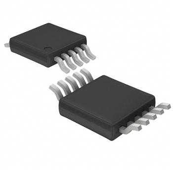
- 封装:10-TFSOP,10-MSOP(0.118",3.00mm 宽)
- RoHS:无铅 / 符合限制有害物质指令(RoHS)规范要求
- 包装方式:带卷 (TR)
- 参考价格:$5.4
更新日期:2024-04-01 00:04:00
产品简介:低功耗、低毛刺脉冲、12 位 DAC
查看详情- 封装:10-TFSOP,10-MSOP(0.118",3.00mm 宽)
- RoHS:无铅 / 符合限制有害物质指令(RoHS)规范要求
- 包装方式:带卷 (TR)
- 参考价格:$5.4
DAC7554IDGSR 供应商
- 公司
- 型号
- 品牌
- 封装/批号
- 数量
- 地区
- 日期
- 说明
- 询价
-
DAC7554IDGSR
原装现货 -
TI
-
-
21+ -
5000
-
深圳
-
12-10
-
只做原装20年老牌供应商,现货请私聊
-
TI
-
原厂原装
22+ -
3288
-
上海市
-
-
-
一级代理原装
-
TI/德州仪器
-
MSOP10
21+ -
10000
-
杭州
-
-
-
只做原装现货,大量现货热卖
-
Texas Instruments
-
原厂原装
22+授权代理 -
15800
-
上海市
-
-
-
旋尔只做进口原装,假一赔十...
-
TI(德州仪器)
-
MSOP10
2022+ -
3219
-
上海市
-
-
-
原装可开发票
-
TI/BB
-
MSOP-10
22+ -
5000
-
常州
-
-
-
主打XILINX品牌价格优势
-
TI
-
MSOP-10
23+ -
5800
-
上海市
-
-
-
进口原装现货,杜绝假货。
DAC7554IDGSR 中文资料属性参数
- 产品培训模块:Data Converter Basics
- 标准包装:2,500
- 类别:集成电路 (IC)
- 家庭:数据采集 - 数模转换器
- 系列:-
- 设置时间:5µs
- 位数:12
- 数据接口:串行,SPI?
- 转换器数目:4
- 电压电源:单电源
- 功率耗散(最大):3.5mW
- 工作温度:-40°C ~ 105°C
- 安装类型:表面贴装
- 封装/外壳:10-TFSOP,10-MSOP(0.118",3.00mm 宽)
- 供应商设备封装:10-MSOP
- 包装:带卷 (TR)
- 输出数目和类型:4 电压,单极
- 采样率(每秒):*
- 配用:296-17893-ND - EVALUATION MODULE FOR DAC7554
产品特性
- 2.7-V to 5.5-V Single Supply
- 12-Bit Linearity and Monotonicity
- Rail-to-Rail Voltage Output
- Settling Time: 5 µs (Max)
- Ultra-Low Glitch Energy: 0.1 nVs
- Ultra-Low Crosstalk: –100 dB
- Low Power: 800 µA (Max)
- Per-Channel Power Down: 1 µA (Max)
- Power-On Reset to Zero Scale
- SPI-Compatible Serial Interface: Up to 50 MHz
- Simultaneous or Sequential Update
- Specified Temperature Range: –40°C to 105°C
- Small 10-Lead MSOP Package
- APPLICATIONS Portable Battery-Powered Instruments Digital Gain and Offset Adjustment Programmable Voltage and Current Sources Programmable Attenuators Industrial Process Control
- Portable Battery-Powered Instruments
- Digital Gain and Offset Adjustment
- Programmable Voltage and Current Sources
- Programmable Attenuators
- Industrial Process Control
产品概述
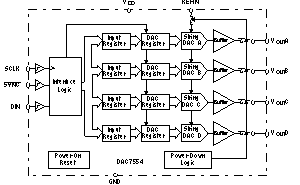
The DAC7554 is a quad-channel, voltage-output DAC with exceptional linearity and monotonicity. Its proprietary architecture also minimizes undesired transients such as code-to-code glitch and channel-to-channel crosstalk. The low-power DAC7554 operates from a single 2.7-V to 5.5-V supply. The DAC7554 output amplifiers can drive a 2-k, 200-pF load rail-to-rail with 5-µs settling time; the output range is set using an external voltage reference.The 3-wire serial interface operates at clock rates up to 50 MHz and is compatible with standard SPI, QSPI, Microwire, and DSP interface standards. The outputs of all DACs may be updated simultaneously or sequentially. The parts incorporate a power-on-reset circuit to ensure that the DAC outputs power up to zero volts and remain there until a valid write cycle to the device takes place. The parts contain a power-down feature that reduces the current consumption of the device to under 1 µA.The small size and low-power operation makes the DAC7554 ideally suited for battery-operated portable applications. The power consumption is typically 3.5 mW at 5 V, 1.65 mW at 3 V, and reduces to 1 µW in power-down mode.The DAC7554 is available in a 10-lead MSOP package and is specified over –40°C to 105°C.
DAC7554IDGSR 数据手册
| 数据手册 | 说明 | 数量 | 操作 |
|---|---|---|---|
 DAC7554IDGSR DAC7554IDGSR
|
12-BIT, QUAD, ULTRALOW GLITCH, VOLTAGE OUTPUT DIGITAL-TO-ANALOG CONVERTER |
21 Pages页,1.05M | 查看 |
DAC7554IDGSR 电路图
DAC7554IDGSR 电路图
DAC7554IDGSR 相关产品
- AD1833AASTZ
- AD1851RZ-J
- AD1851RZ-REEL7
- AD1852JRSZRL
- AD1856RZ
- AD1859JRZ-RL
- AD1866RZ-REEL
- AD1933WBSTZ
- AD1934WBSTZ
- AD1953YSTZ
- AD1954YSTZ
- AD1954YSTZRL
- AD1955ARSZ
- AD1955ARSZRL
- AD420AR-32-REEL
- AD420ARZ-32
- AD420ARZ-32-REEL
- AD421BR
- AD421BRZ
- AD421BRZRL
- AD421BRZRL7
- AD5024BRUZ
- AD5024BRUZ-REEL7
- AD5025BRUZ
- AD5040BRJZ-REEL7
- AD5044BRUZ
- AD5060ARJZ-2REEL7
- AD5060BRJZ-1500RL7
- AD5060BRJZ-1REEL7
- AD5060BRJZ-2500RL7