 搜索
搜索
 发布采购
发布采购
- 封装:12-UFDFN 裸露焊盘
- RoHS:无铅 / 符合限制有害物质指令(RoHS)规范要求
- 包装方式:带卷 (TR)
- 参考价格:$1.85625-$1.96764
更新日期:2024-04-01 00:04:00

产品简介:12 位超低短时脉冲波形干扰电压输出数模转换器
查看详情- 封装:12-UFDFN 裸露焊盘
- RoHS:无铅 / 符合限制有害物质指令(RoHS)规范要求
- 包装方式:带卷 (TR)
- 参考价格:$1.85625-$1.96764
DAC7551IDRNTG4 供应商
- 公司
- 型号
- 品牌
- 封装/批号
- 数量
- 地区
- 日期
- 说明
- 询价
-
TI
-
原厂原装
22+ -
3288
-
上海市
-
-
-
一级代理原装
DAC7551IDRNTG4 中文资料属性参数
- 产品培训模块:Data Converter Basics
- 标准包装:250
- 类别:集成电路 (IC)
- 家庭:数据采集 - 数模转换器
- 系列:-
- 设置时间:5µs
- 位数:12
- 数据接口:DSP,MICROWIRE?,QSPI?,串行,SPI?
- 转换器数目:1
- 电压电源:单电源
- 功率耗散(最大):-
- 工作温度:-40°C ~ 105°C
- 安装类型:表面贴装
- 封装/外壳:12-UFDFN 裸露焊盘
- 供应商设备封装:12-USON(3x2)
- 包装:带卷 (TR)
- 输出数目和类型:1 电压,单极
- 采样率(每秒):500k
产品特性
- Relative Accuracy (INL): ±0.35LSB
- Ultra-Low Glitch Energy: 0.1nV-s
- Low Power Operation: 100µA at 2.7V
- Power-On Reset to Zero Scale
- Power Supply: 2.7V to 5.5V Single Supply
- Power-Down: 0.05µA at 2.7V
- 12-Bit Linearity and Monotonicity
- Rail-to-Rail Voltage Output
- Settling Time: 5µs (Max)
- SPI-Compatible Serial Interface with Schmitt-Trigger Input: Up to 50MHz
- Daisy-Chain Capability
- Asynchronous Hardware Clear to Zero Scale
- Specified Temperature Range: -40°C to +105°C
- Small, 2 x 3 mm, 12-Lead SON Package
- APPLICATIONSPortable, Battery-Powered InstrumentsDigital Gain and Offset AdjustmentProgrammable Voltage and Current SourcesProgrammable AttenuatorsIndustrial Process Control
- Portable, Battery-Powered Instruments
- Digital Gain and Offset Adjustment
- Programmable Voltage and Current Sources
- Programmable Attenuators
- Industrial Process Control
产品概述
The DAC7551 is a single-channel, voltage-output digital-to-analog converter (DAC) with exceptional linearity and monotonicity, and a proprietary architecture that minimizes glitch energy. The low-power DAC7551 operates from a single 2.7V to 5.5V supply. The DAC7551 output amplifiers can drive a 2k, 200pF load rail-to-rail with 5µs settling time; the output range is set using an external voltage reference.The 3-wire serial interface operates at clock rates up to 50MHz and is compatible with SPI™, QSPI™, Microwire™, and DSP interface standards. The parts incorporate a power-on-reset circuit to ensure that the DAC output powers up to 0V and remains there until a valid write cycle to the device takes place. The part contains a power-down feature that reduces the current consumption of the device to under 2µA. Small size and low-power operation make the DAC7551 ideally suited for battery-operated, portable applications. The power consumption is typically 0.5mW at 5V, 0.23mW at 3V, and reduces to 1µW in power-down mode. The DAC7551 is available in a 12-lead SON package and is specified over -40°C to +105°C.
DAC7551IDRNTG4 电路图
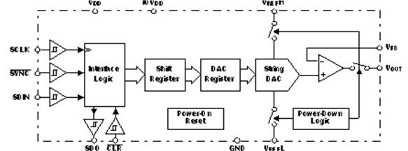
DAC7551IDRNTG4 电路图
DAC7551IDRNTG4 相关产品
- AD1833AASTZ
- AD1851RZ-J
- AD1851RZ-REEL7
- AD1852JRSZRL
- AD1856RZ
- AD1859JRZ-RL
- AD1866RZ-REEL
- AD1933WBSTZ
- AD1934WBSTZ
- AD1953YSTZ
- AD1954YSTZ
- AD1954YSTZRL
- AD1955ARSZ
- AD1955ARSZRL
- AD420AR-32-REEL
- AD420ARZ-32
- AD420ARZ-32-REEL
- AD421BR
- AD421BRZ
- AD421BRZRL
- AD421BRZRL7
- AD5024BRUZ
- AD5024BRUZ-REEL7
- AD5025BRUZ
- AD5040BRJZ-REEL7
- AD5044BRUZ
- AD5060ARJZ-2REEL7
- AD5060BRJZ-1500RL7
- AD5060BRJZ-1REEL7
- AD5060BRJZ-2500RL7