 搜索
搜索
 发布采购
发布采购
- 封装:100-TQFP 裸露焊盘
- RoHS:无铅 / 符合限制有害物质指令(RoHS)规范要求
- 包装方式:托盘
- 参考价格:$32.04-$49.4
更新日期:2024-04-01 00:04:00

产品简介:双通道、16 位、500MSPS、1x-16x 内插数模转换器 (DAC)
查看详情- 封装:100-TQFP 裸露焊盘
- RoHS:无铅 / 符合限制有害物质指令(RoHS)规范要求
- 包装方式:托盘
- 参考价格:$32.04-$49.4
DAC5686IPZP 供应商
- 公司
- 型号
- 品牌
- 封装/批号
- 数量
- 地区
- 日期
- 说明
- 询价
-
TI
-
原厂原装
22+ -
3288
-
上海市
-
-
-
一级代理原装
-
TI
-
-
2019+ -
5800
-
上海市
-
-
-
全新原装现货
-
TI(德州仪器)
-
HTQFP-100(14x14)
2022+ -
12000
-
上海市
-
-
-
原装可开发票
-
TI
-
TQFP100
21+ -
5000
-
上海市
-
-
-
原装现货,品质为先,请来电垂询!
-
TI
-
HTQFP
新批号 -
887000
-
上海市
-
-
-
原厂发货进口原装微信同步QQ893727827
-
TI
-
TQFP
23+ -
5800
-
上海市
-
-
-
进口原装现货,杜绝假货。
-
TI
-
QFP
- -
8
-
台州
-
-
DAC5686IPZP 中文资料属性参数
- 产品培训模块:Data Converter Basics
- 标准包装:90
- 类别:集成电路 (IC)
- 家庭:数据采集 - 数模转换器
- 系列:-
- 设置时间:12ns
- 位数:16
- 数据接口:并联
- 转换器数目:2
- 电压电源:模拟和数字
- 功率耗散(最大):950mW
- 工作温度:-40°C ~ 85°C
- 安装类型:表面贴装
- 封装/外壳:100-TQFP 裸露焊盘
- 供应商设备封装:100-HTQFP(14x14)
- 包装:托盘
- 输出数目和类型:4 电流,单极
- 采样率(每秒):500M
- 配用:296-31328-ND - MODULE PATTERN GENERATOR BOARD296-17515-ND - EVALUATION MODULE FOR DAC5686
- 其它名称:296-16695-5
产品特性
- 500-MSPS Maximum-Update-Rate DAC
- WCDMA ACPR 1 Carrier: 76 dB Centered at 30.72-MHz IF, 245.76 MSPS 1 Carrier: 73 dB Centered at 61.44-MHz IF, 245.76 MSPS 2 Carrier: 72 dB Centered at 30.72-MHz IF, 245.76 MSPS 4 Carrier: 64 dB Centered at 92.16-MHz IF, 491.52 MSPS
- 1 Carrier: 76 dB Centered at 30.72-MHz IF, 245.76 MSPS
- 1 Carrier: 73 dB Centered at 61.44-MHz IF, 245.76 MSPS
- 2 Carrier: 72 dB Centered at 30.72-MHz IF, 245.76 MSPS
- 4 Carrier: 64 dB Centered at 92.16-MHz IF, 491.52 MSPS
- Selectable 2×, 4×, 8×, and 16× Interpolation Linear Phase 0.05-dB Pass-Band Ripple 80-dB Stop-Band Attenuation Stop-Band Transition 0.4-0.6 fDATA
- Linear Phase
- 0.05-dB Pass-Band Ripple
- 80-dB Stop-Band Attenuation
- Stop-Band Transition 0.4-0.6 fDATA
- 32-Bit Programmable NCO
- On-Chip 2× - 16× PLL Clock Multiplier With Bypass Mode
- Differential Scalable Current Outputs: 2 mA to 20 mA
- On-Chip 1.2-V Reference
- 1.8-V Digital and 3.3-V Analog Supplies
- 1.8-V/3.3-V CMOS-Compatible Interface
- Power Dissipation: 950 mW at Full Maximum Operating Conditions
- Package: 100-Pin HTQFP
- APPLICATIONS Cellular Base Transceiver Station Transmit Channel CDMA: W-CDMA, CDMA2000, IS-95 TDMA: GSM, IS-136, EDGE/UWC-136 Baseband I and Q Transmit Input Interface: Quadrature Modulation for Interfacing With Baseband Complex Mixing ASICs Single-Sideband Up-Conversion Diversity Transmit Cable Modem Termination System
- Cellular Base Transceiver Station Transmit Channel CDMA: W-CDMA, CDMA2000, IS-95 TDMA: GSM, IS-136, EDGE/UWC-136
- CDMA: W-CDMA, CDMA2000, IS-95
- TDMA: GSM, IS-136, EDGE/UWC-136
- Baseband I and Q Transmit
- Input Interface: Quadrature Modulation for Interfacing With Baseband Complex Mixing ASICs
- Single-Sideband Up-Conversion
- Diversity Transmit
- Cable Modem Termination System
产品概述
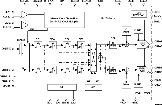
The DAC5686 is a dual-channel 16-bit high-speed
digital-to-analog converter (DAC) with integrated 2×, 4×, 8×, and 16×
interpolation filters, a numerically controlled oscillator (NCO), onboard clock
multiplier, and on-chip voltage reference. The DAC5686 has been specifically
designed to allow for low input data rates between the DAC and ASIC, or FPGA,
and high output transmit intermediate frequencies (IF). Target applications
include high-speed digital data transmission in wired and wireless
communication systems and high-frequency direct-digital synthesis DDS.The DAC5686 provides three modes of operation: dual-channel,
single-sideband, and quadrature modulation. In dual-channel mode, interpolation
filtering increases the DAC update rate, which reduces sinx/x rolloff and
enables the use of relaxed analog post-filtering.Single-sideband mode provides an alternative interface to
the analog quadrature modulators. Channel carrier selection is performed at
baseband by mixing in the ASIC/FPGA. Baseband I and Q from the ASIC/FPGA are
input to the DAC5686, which in turn performs a complex mix resulting in Hilbert
transform pairs at the outputs of the DAC5686's two DACs. An external RF
quadrature modulator then performs the final single-sideband up-conversion. The
DAC5686's complex mixing frequencies are flexibly chosen with the 32-bit
programmable NCO.Unmatched gains and offsets at the RF quadrature modulator
result in unwanted sideband and local oscillator feedthrough. Each DAC in the
DAC5686 has an 11-bit offset adjustment and 12-bit gain adjustment, which
compensate for quadrature modulator input imbalances, thus reducing RF
filtering requirements.In quadrature modulation mode, on-chip mixing provides
baseband-to-IF up-conversion. Mixing frequencies are flexibly chosen with a
32-bit programmable NCO. Channel carrier selection is performed at baseband by
complex mixing in the ASIC/FPGA. Baseband I and Q from the ASIC/FPGA are input
to the DAC5686, which interpolates the low data-rate signal to higher data
rates. The single DAC output from the DAC5686 is the final IF single-sideband
spectrum presented to RF.The 2×, 4×, 8×, and 16× interpolation filters are
implemented as a cascade of half-band 2× interpolation filters. Unused filters
for interpolation rates of less than 16× are shut off to reduce power
consumption. The DAC5686 provides a full bypass mode, which enables the user to
bypass all the interpolation and mixing.The DAC5686 PLL clock multiplier controls all internal
clocks for the digital filters and the DAC cores. The differential clock input
and internal clock circuitry provides for optimum jitter performance. Sine wave
clock input signal is supported. The PLL can be bypassed by an external clock
running at the DAC core update rate. The clock divider of the PLL ensures that
the digital filters operate at the correct clock frequencies.The DAC5686 operates with an analog supply voltage of 3.3 V
and a digital supply voltage of 1.8 V. Digital I/Os are 1.8-V and 3.3-V CMOS
compatible. Power dissipation is 950 mW at maximum operating conditions. The
DAC5686 provides a nominal full-scale differential current output of 20 mA,
supporting both single-ended and differential applications. The output current
can be directly fed to the load with no additional external output buffer
required. The device has been specifically designed for a differential
transformer-coupled output with a 50- doubly terminated load. For a 20-mA
full-scale output current, both a 4:1 impedance ratio (resulting in an output
power of 4 dBm) and 1:1 impedance ratio transformer (-2-dBm output power)
are supported.The DAC5686 operational modes are configured by programming
registers through a serial interface. The serial interface can be configured to
either a 3- or 4-pin interface allowing it to communicate with many
industry-standard microprocessors and microcontrollers. Data (I and Q) can be
input to the DAC5686 as separate parallel streams on two data buses, or as a
single interleaved data stream on one data bus.An accurate on-chip 1.2-V temperature-compensated band-gap
reference and control amplifier allows the user to adjust the full-scale output
current from 20 mA down to 2 mA. This provides 20-dB gain range control
capabilities. Alternatively, an external reference voltage can be applied for
maximum flexibility. The device features a SLEEP mode, which reduces the
standby power to approximately 10 mW, thereby minimizing the system power
consumption.The DAC5686 is available in a 100-pin HTQFP package. The
device is characterized for operation over the industrial temperature range of
-40°C to 85°C.
DAC5686IPZP 数据手册
| 数据手册 | 说明 | 数量 | 操作 |
|---|---|---|---|
 DAC5686IPZP DAC5686IPZP
|
16-BIT, 500-MSPS, 2X16X INTERPOLATING DUAL-CHANNEL DIGITAL-TO-ANALOG CONVERTER |
46 Pages页,1.32M | 查看 |
DAC5686IPZP 电路图
DAC5686IPZP 电路图
DAC5686IPZP 相关产品
- AD1833AASTZ
- AD1851RZ-J
- AD1851RZ-REEL7
- AD1852JRSZRL
- AD1856RZ
- AD1859JRZ-RL
- AD1866RZ-REEL
- AD1933WBSTZ
- AD1934WBSTZ
- AD1953YSTZ
- AD1954YSTZ
- AD1954YSTZRL
- AD1955ARSZ
- AD1955ARSZRL
- AD420AR-32-REEL
- AD420ARZ-32
- AD420ARZ-32-REEL
- AD421BR
- AD421BRZ
- AD421BRZRL
- AD421BRZRL7
- AD5024BRUZ
- AD5024BRUZ-REEL7
- AD5025BRUZ
- AD5040BRJZ-REEL7
- AD5044BRUZ
- AD5060ARJZ-2REEL7
- AD5060BRJZ-1500RL7
- AD5060BRJZ-1REEL7
- AD5060BRJZ-2500RL7