 搜索
搜索
 发布采购
发布采购
- 封装:48-TQFP 裸露焊盘
- RoHS:无铅 / 符合限制有害物质指令(RoHS)规范要求
- 包装方式:托盘
- 参考价格:$44.21252
更新日期:2024-04-01 00:04:00

产品简介:14 位、400MSPS 数模转换器 (DAC)
查看详情- 封装:48-TQFP 裸露焊盘
- RoHS:无铅 / 符合限制有害物质指令(RoHS)规范要求
- 包装方式:托盘
- 参考价格:$44.21252
DAC5675AIPHP 供应商
- 公司
- 型号
- 品牌
- 封装/批号
- 数量
- 地区
- 日期
- 说明
- 询价
-
TI
-
原厂原装
22+ -
3288
-
上海市
-
-
-
一级代理原装
-
TI
-
-
2019+ -
3000
-
上海市
-
-
-
全新原装现货
-
TI(德州仪器)
-
HTQFP-48(7x7)
2022+ -
12000
-
上海市
-
-
-
原装可开发票
-
TI
-
QFP
新批号 -
887000
-
上海市
-
-
-
原厂发货进口原装微信同步QQ893727827
-
TI
-
LQFP48
23+ -
5800
-
上海市
-
-
-
进口原装现货,杜绝假货。
DAC5675AIPHP 中文资料属性参数
- 产品培训模块:Data Converter Basics
- 标准包装:250
- 类别:集成电路 (IC)
- 家庭:数据采集 - 数模转换器
- 系列:-
- 设置时间:-
- 位数:14
- 数据接口:并联
- 转换器数目:1
- 电压电源:模拟和数字
- 功率耗散(最大):900mW
- 工作温度:-40°C ~ 85°C
- 安装类型:表面贴装
- 封装/外壳:48-TQFP 裸露焊盘
- 供应商设备封装:48-HTQFP(7x7)
- 包装:托盘
- 输出数目和类型:2 电流,单极
- 采样率(每秒):400M
- 配用:296-30861-ND - EVAL MODULE FOR DAC5675
- 其它名称:296-18215
产品特性
- 400MSPS Update Rate
- LVDS-Compatible Input Interface
- Spurious-Free Dynamic Range (SFDR) to Nyquist: 69dBc at 70MHz IF, 400MSPS
- 69dBc at 70MHz IF, 400MSPS
- W-CDMA Adjacent Channel Power Ratio (ACPR): 73dBc at 30.72MHz IF, 122.88MSPS 71dBc at 61.44MHz IF, 245.76MSPS
- 73dBc at 30.72MHz IF, 122.88MSPS
- 71dBc at 61.44MHz IF, 245.76MSPS
- Differential Scalable Current Sink Outputs: 2mA to 20mA
- On-Chip 1.2V Reference
- Single 3.3V Supply Operation
- Power Dissipation: 660mW at fCLK = 400MSPS, fOUT = 20MHz
- Package: 48-Pin HTQFP PowerPad, TJA = 28.8°C/W
产品概述
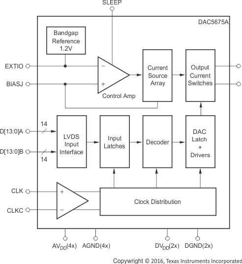
The DAC5675A is a 14-bit resolution high-speed digital-to-analog converter. The DAC5675A
is designed for high-speed digital data transmission in wired and wireless communication systems,
high-frequency direct-digital synthesis (DDS), and waveform reconstruction in test and measurement
applications. The DAC5675A has excellent spurious-free dynamic range (SFDR) at high intermediate
frequencies, which makes the DAC5675A well-suited for multicarrier transmission in TDMA- and
CDMA-based cellular base transceiver stations (BTSs).The DAC5675A operates from a single-supply voltage of 3.3 V. Power dissipation is 660 mW
at
fCLK = 400 MSPS, fOUT = 70 MHz. The DAC5675A
provides a nominal full-scale differential current output of 20mA, supporting both single-ended and
differential applications. The output current can be directly fed to the load with no additional
external output buffer required. The output is referred to the analog supply voltage
AVDD.The DAC5675A comprises a low-voltage differential signaling (LVDS) interface for
high-speed digital data input. LVDS features a low differential voltage swing with a low constant
power consumption across frequency, allowing for high-speed data transmission with low noise
levels; that is, with low electromagnetic interference (EMI). LVDS is typically implemented in
low-voltage digital CMOS processes, making it the ideal technology for high-speed interfacing
between the DAC5675A and high-speed low-voltage CMOS ASICs or FPGAs. The DAC5675A
current-sink-array architecture supports update rates of up to 400MSPS. On-chip edge-triggered
input latches provide for minimum setup and hold times, thereby relaxing interface timing.The DAC5675A has been specifically designed for a differential transformer-coupled output
with a 50 Ω doubly- terminated load. With the 20 mA full-scale output current, both a 4:1 impedance
ratio (resulting in an output power of 4 dBm) and 1:1 impedance ratio transformer (–2 dBm) are
supported. The last configuration is preferred for optimum performance at high output frequencies
and update rates. The outputs are terminated to AVDD and have voltage compliance ranges from
AVDD –1 to AVDD + 0.3 V.An accurate on-chip 1.2-V temperature-compensated bandgap reference and control amplifier
allows the user to adjust this output current from 20 mA down to 2 mA. This provides 20-dB gain
range control capabilities. Alternatively, an external reference voltage may be applied. The
DAC5675A features a SLEEP mode, which reduces the standby power to approximately 18 mW.The DAC5675A is available in a 48-pin HTQFP thermally-enhanced PowerPad package. This
package increases thermal efficiency in a standard size IC package. The device is characterized for
operation over the industrial temperature range of –40°C to +85°C.
DAC5675AIPHP 数据手册
| 数据手册 | 说明 | 数量 | 操作 |
|---|---|---|---|
 DAC5675AIPHP DAC5675AIPHP
|
14-Bit, 400-MSPS Digital-to-Analog Converter 48-HTQFP -40 to 85 |
25页,983K | 查看 |
DAC5675AIPHP 电路图
DAC5675AIPHP 电路图
DAC5675AIPHP 相关产品
- AD1833AASTZ
- AD1851RZ-J
- AD1851RZ-REEL7
- AD1852JRSZRL
- AD1856RZ
- AD1859JRZ-RL
- AD1866RZ-REEL
- AD1933WBSTZ
- AD1934WBSTZ
- AD1953YSTZ
- AD1954YSTZ
- AD1954YSTZRL
- AD1955ARSZ
- AD1955ARSZRL
- AD420AR-32-REEL
- AD420ARZ-32
- AD420ARZ-32-REEL
- AD421BR
- AD421BRZ
- AD421BRZRL
- AD421BRZRL7
- AD5024BRUZ
- AD5024BRUZ-REEL7
- AD5025BRUZ
- AD5040BRJZ-REEL7
- AD5044BRUZ
- AD5060ARJZ-2REEL7
- AD5060BRJZ-1500RL7
- AD5060BRJZ-1REEL7
- AD5060BRJZ-2500RL7