 搜索
搜索
 发布采购
发布采购
- 参考价格:¥24,396.74
更新日期:2024-04-01 00:04:00
DAC121S101WGRQV 供应商
- 公司
- 型号
- 品牌
- 封装/批号
- 数量
- 地区
- 日期
- 说明
- 询价
-
TI
-
TEJIA
21+ -
268
-
上海市
-
-
-
原装现货,品质为先,请来电垂询!
DAC121S101WGRQV 中文资料属性参数
- 制造商:National Semiconductor (TI)
- 转换器数量:1
- DAC 输出端数量:1
- 分辨率:12 bit
- 接口类型:Serial (3-Wire, Microwire, QSPI, SPI)
- 稳定时间:15 us
- 最大工作温度:+ 125 C
- 封装 / 箱体:CSOIC
- 封装:Tray
- 最小工作温度:- 55 C
- 输出类型:Voltage
- 工厂包装数量:54
- Supply Voltage - Max:5.5 V
- Supply Voltage - Min:2.7 V
- 电压参考:Supply
产品特性
- 5962R07726 Total Ionizing Dose 100 krad(Si) Single Event Latch-up Immune 120 MeV-cm2/mg Single Event Functional Interrupt Immune 120 MeV-cm2/mg (See Radiation Report)
- Total Ionizing Dose 100 krad(Si)
- Single Event Latch-up Immune 120 MeV-cm2/mg
- Single Event Functional Interrupt Immune 120 MeV-cm2/mg (See Radiation Report)
- Ensured Monotonicity
- Low Power Operation
- Rail-to-Rail Voltage Output
- Power-On Reset to Zero Volts Output
- SYNC Interrupt Facility
- Wide Power Supply Range (2.7 V to 5.5 V)
- Small Packages
- Power-Down Feature
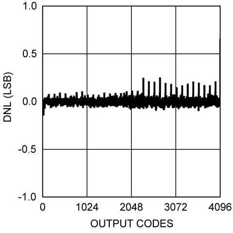
- Key Specifications Resolution: 12 Bits DNL: +0.21, –0.10 LSB (Typical) Output Settling Time: 12.5 µs (Typical) Zero Code Error: 2.1 mV (Typical) Full-Scale Error: –0.04% FS (Typical) Power Dissipation Normal Mode: 0.52 mW (3.6 V) and 1.19 mW (5.5 V) Typical Power-Down Mode: 0.014 µW (3.6 V) and 0.033 µW (5.5 V) Typical
- Resolution: 12 Bits
- DNL: +0.21, –0.10 LSB (Typical)
- Output Settling Time: 12.5 µs (Typical)
- Zero Code Error: 2.1 mV (Typical)
- Full-Scale Error: –0.04% FS (Typical)
- Power Dissipation Normal Mode: 0.52 mW (3.6 V) and 1.19 mW (5.5 V) Typical Power-Down Mode: 0.014 µW (3.6 V) and 0.033 µW (5.5 V) Typical
- Normal Mode: 0.52 mW (3.6 V) and 1.19 mW (5.5 V) Typical
- Power-Down Mode: 0.014 µW (3.6 V) and 0.033 µW (5.5 V) Typical
产品概述
The DAC121S101QML-SP device is a full-featured, general-purpose, 12-bit voltage-output
digital-to-analog converter (DAC) that can operate from a single 2.7-V to 5.5-V supply and consumes
just 177 µA of current at 3.6 V. The on-chip output amplifier allows rail-to-rail output swing and
the three-wire serial interface operates at clock rates up to 20 MHz over the specified supply voltage range and is compatible with standard SPI, QSPI, MICROWIRE, and DSP interfaces.The supply voltage for the DAC121S101QML-SP serves as its voltage reference, providing
the widest possible output dynamic range. A power-on reset circuit ensures that the DAC output
powers up to zero volts and remains there until there is a valid write to the device. A power-down
feature reduces power consumption to less than a microWatt.The low power consumption and small packages of the DAC121S101QML-SP make it an excellent
choice for use in battery-operated equipment.
DAC121S101WGRQV 电路图
DAC121S101WGRQV 电路图
DAC121S101WGRQV 相关产品
- 100301QC
- 100304QC
- 100310QC
- 100311QC
- 100313QC
- 100316QC
- 100322QC
- 100329APC
- 100329DC
- 100336DC
- 100336PC
- 100341QC
- 100351DC
- 100351PC
- 100363QC
- 100364QC
- 100370QC
- 100390QC
- 100398QI
- 11AA010T-I/TT
- 11AA160T-I/TT
- 11LC010T-I/TT
- 11LC020T-I/TT
- 11LC040T-E/TT
- 11LC160T-E/TT
- 1ED020I12-F
- 2304NZGI-1LF
- 23A640-I/SN
- 23K256-I/SN
- 23K256-I/ST