 搜索
搜索
 发布采购
发布采购
- 参考价格:¥10.01
更新日期:2024-04-01 00:04:00

DAC121S101CIMKX 供应商
- 公司
- 型号
- 品牌
- 封装/批号
- 数量
- 地区
- 日期
- 说明
- 询价
-
TI
-
原厂原装
22+ -
3288
-
上海市
-
-
-
一级代理原装
-
TI(德州仪器)
-
SOT-23-THIN-6
2022+ -
12
-
上海市
-
-
-
原装可开发票
-
TI
-
SOT23-6
21+ -
50000
-
上海市
-
-
-
原装现货!品质为先!请来电垂询!
-
TI
-
原厂原封装
新批号 -
887000
-
上海市
-
-
-
原厂发货进口原装微信同步QQ893727827
DAC121S101CIMKX 中文资料属性参数
- 制造商:National Semiconductor (TI)
- 转换器数量:1
- DAC 输出端数量:1
- 分辨率:12 bit
- 接口类型:Serial (3-Wire, Microwire, QSPI, SPI)
- 稳定时间:10 us
- 最大工作温度:+ 105 C
- 封装 / 箱体:TSOT
- 封装:Reel
- 最小工作温度:- 40 C
- 输出类型:Voltage
- 工厂包装数量:3000
- Supply Voltage - Max:5.5 V
- Supply Voltage - Min:2.7 V
- 电压参考:Supply
产品特性
- DAC121S101-Q1 is AEC-Q100 Grade 1 Qualified and is Manufactured on an Automotive Grade Flow.
- Ensured Monotonicity
- Low Power Operation
- Rail-to-Rail Voltage Output
- Power-on Reset to Zero Volts Output
- Wide Temperature Range of –40°C to +125°C
- Wide Power Supply Range of 2.7 V to 5.5 V
- Small Packages
- Power Down Feature
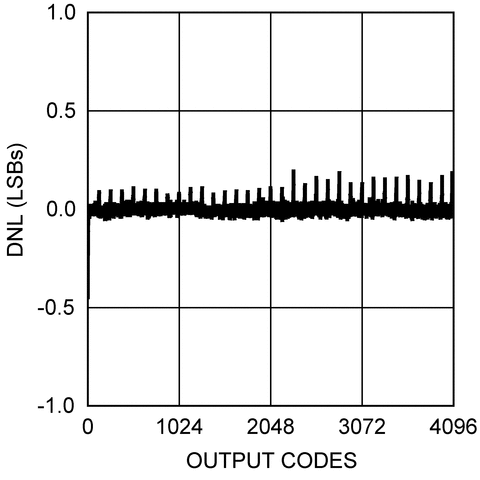
- Key Specifications 12-Bit Resolution DNL -0.15, +0.25 LSB (Typical) 8-µs Output Settling Time (Typical) 4-mV Zero Code Error (Typical) Full-Scale Error at –0.06 %FS (Typical) 0.64-mW (3.6-V) / 1.43-mW (5.5-V) Normal Mode Power Consumption (Typical) 0.14-µW (3.6-V) / 0.39-µW (5.5-V) Power- Down Mode (Typical)
- 12-Bit Resolution
- DNL -0.15, +0.25 LSB (Typical)
- 8-µs Output Settling Time (Typical)
- 4-mV Zero Code Error (Typical)
- Full-Scale Error at –0.06 %FS (Typical)
- 0.64-mW (3.6-V) / 1.43-mW (5.5-V) Normal Mode Power Consumption (Typical)
- 0.14-µW (3.6-V) / 0.39-µW (5.5-V) Power- Down Mode (Typical)
- Battery-Powered Instruments
- Digital Gain and Offset Adjustment
- Programmable Voltage and Current Sources
- Programmable Attenuators
- Automotive
产品概述
The DAC121S101 device is a full-featured, general-purpose, 12-bit voltage-output
digital-to-analog converter (DAC) that can operate from a single 2.7-V to 5.5-V supply and consumes
just 177 µA of current at 3.6 V. The on-chip output amplifier allows rail-to-rail output swing and
the three wire serial interface operates at clock rates up to 30 MHz over the specified supply
voltage range and is compatible with standard SPI™, QSPI, MICROWIRE and DSP interfaces. Competitive devices are
limited to 20-MHz clock rates at supply voltages in the 2.7 V to 3.6 V range.The supply voltage for the DAC121S101 serves as its voltage reference, providing the
widest possible output dynamic range. A power-on reset circuit ensures that the DAC output powers
up to zero volts and remains there until there is a valid write to the device. A power-down feature
reduces power consumption to less than a microWatt.The low power consumption and small packages of the DAC121S101 make it an excellent
choice for use in battery operated equipment.The DAC121S101 is a direct replacement for the AD5320 and the DAC7512 and is one of a
family of pin compatible DACs, including the 8-bit DAC081S101 and the 10-bit DAC101S101. The
DAC121S101 operates over the extended industrial temperature range of &–40®C to +104M7 natural dad while the
DAC121S101-Q1 operates over the Grade 1 automotive temperature range of –40°C to +125°C. The
DAC121S101 is available in a 6-lead SOT and an 8-lead VSSOP and the DAC121S101-Q1 is available in
the 6-lead SOT only.
DAC121S101CIMKX 数据手册
| 数据手册 | 说明 | 数量 | 操作 |
|---|---|---|---|
 DAC121S101CIMKX DAC121S101CIMKX
|
12-Bit Micro Power Digital-to-Analog Converter with Rail-to-Rail Output |
19 Pages页,908K | 查看 |
DAC121S101CIMKX 电路图
DAC121S101CIMKX 电路图
DAC121S101CIMKX 相关产品
- 100301QC
- 100304QC
- 100310QC
- 100311QC
- 100313QC
- 100316QC
- 100322QC
- 100329APC
- 100329DC
- 100336DC
- 100336PC
- 100341QC
- 100351DC
- 100351PC
- 100363QC
- 100364QC
- 100370QC
- 100390QC
- 100398QI
- 11AA010T-I/TT
- 11AA160T-I/TT
- 11LC010T-I/TT
- 11LC020T-I/TT
- 11LC040T-E/TT
- 11LC160T-E/TT
- 1ED020I12-F
- 2304NZGI-1LF
- 23A640-I/SN
- 23K256-I/SN
- 23K256-I/ST