 搜索
搜索
 发布采购
发布采购
更新日期:2024-04-01 00:04:00

产品简介:具有轨到轨输出的汽车类 10 位微功耗 4 通道数模转换器 (DAC)
查看详情DAC104S085QIMM/NOPB 供应商
- 公司
- 型号
- 品牌
- 封装/批号
- 数量
- 地区
- 日期
- 说明
- 询价
-
TI
-
原厂原装
22+ -
3288
-
上海市
-
-
-
一级代理原装
-
TI(德州仪器)
-
MSOP-10
2022+ -
12000
-
上海市
-
-
-
原装可开发票
DAC104S085QIMM/NOPB 中文资料属性参数
- 现有数量:774现货1,000Factory
- 价格:1 : ¥50.56000剪切带(CT)1,000 : ¥30.27720卷带(TR)
- 系列:Automotive, AEC-Q100
- 包装:卷带(TR)剪切带(CT)Digi-Reel? 得捷定制卷带
- 产品状态:在售
- Digi-Key Programmable:Not Verified
- 位数:10
- 数模转换器数:4
- 建立时间:6μs
- 输出类型:Voltage - Buffered
- 差分输出:无
- 数据接口:SPI,DSP
- 参考类型:外部
- 电压 - 供电,模拟:2.7V ~ 5.5V
- 电压 - 供电,数字:2.7V ~ 5.5V
- INL/DNL (LSB):±0.7,+0.08/-0.03
- 架构:电阻串 DAC
- 工作温度:-40°C ~ 125°C
- 封装/外壳:10-TFSOP,10-MSOP(0.118",3.00mm 宽)
- 供应商器件封装:10-VSSOP
- 安装类型:表面贴装型
产品特性
- Qualified for Automotive Applications
- AEC-Q100 Qualified With the Following Results: Device Temperature Grade 1: –40°C to 125°C Ambient Operating Temperature
- Device Temperature Grade 1: –40°C to 125°C Ambient Operating Temperature
- Ensured Monotonicity
- Low Power Operation
- Rail-to-Rail Voltage Output
- Power-On Reset to 0 V
- Simultaneous Output Updating
- Wide Power Supply Range (2.7 V to 5.5 V)
- Key Specifications Resolution: 10 bits INL: ±2 LSB (Maximum) DNL: +0.35 / –0.25 LSB (Maximum) Settling Time: 6 µs (Maximum) Zero Code Error: 15 mV (Maximum) Full-Scale Error: –0.75% FS (Maximum) Typical Supply Power Normal Mode: 1.1 mW (3 V), 2.5 mW (5 V) Power Down: 0.3 µW (3 V), 0.8µW (5 V)
- Resolution: 10 bits
- INL: ±2 LSB (Maximum)
- DNL: +0.35 / –0.25 LSB (Maximum)
- Settling Time: 6 µs (Maximum)
- Zero Code Error: 15 mV (Maximum)
- Full-Scale Error: –0.75% FS (Maximum)
- Typical Supply Power Normal Mode: 1.1 mW (3 V), 2.5 mW (5 V) Power Down: 0.3 µW (3 V), 0.8µW (5 V)
- Normal Mode: 1.1 mW (3 V), 2.5 mW (5 V)
- Power Down: 0.3 µW (3 V), 0.8µW (5 V)
产品概述
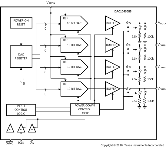
The DAC104S085 device is a full-featured, general-purpose QUAD 10-bit voltage-output
digital-to-analog converter (DAC) that can operate from a single 2.7-V to 5.5-V supply and consumes
1.1 mW at 3 V and
2.5 mW at 5 V. The DAC104S085 is packaged in 10-pin SON and VSSOP packages. The 10-pin SON
package makes the DAC104S085 the smallest QUAD DAC in its class. The on-chip output amplifier
allows rail-to-rail output swing and the three wire serial interface operates at clock rates up to
40 MHz over the entire supply voltage range. Competitive devices are limited to 25-MHz clock rates
at supply voltages in the 2.7-V to 3.6-V range. The serial interface is compatible with standard
SPI, QSPI, MICROWIRE, and DSP interfaces.The reference for the DAC104S085 serves all four channels and can vary in voltage between
1 V and VA, providing the widest possible output dynamic range. The
DAC104S085 has a 16-bit input shift register that controls the outputs to be updated, the mode of
operation, the power-down condition, and the binary input data. All four outputs can be updated
simultaneously or individually depending on the setting of the two mode of operation bits.A power-on reset circuit ensures that the DAC output powers up to zero volts and remains
there until there is a valid write to the device. A power-down feature reduces power consumption to
less than a microWatt with three different termination options.The low power consumption and small packages of the DAC104S085 make it an excellent
choice for use in battery-operated equipment.The DAC104S085 is one of a family of pin-compatible DACs, including the 8-bit DAC084S085
and the 12-bit DAC124S085. The DAC104S085 operates over the extended industrial temperature range
of –40°C to +125°C.
DAC104S085QIMM/NOPB 电路图
DAC104S085QIMM/NOPB 电路图
DAC104S085QIMM/NOPB 相关产品
- 5962-0720401VXC
- 5962-0720801VXC
- 5962-87802012A
- 5962-9152101MXA
- 5962-9961601HXA
- 6PA3100IRHBRQ1
- AD2S1210SST-EP-RL7
- AD2S1210WDSTZ
- AD2S80ATD/B
- AD3421QRWERQ1
- AD3421QRWETQ1
- AD5122ABCPZ100-RL7
- AD5122BCPZ100-RL7
- AD5122BRUZ10
- AD5123BCPZ100-RL7
- AD5142BCPZ10-RL7
- AD5235BRU25-EP-RL7
- AD5317RBRUZ
- AD5317RBRUZ-RL7
- AD5372BCPZ
- AD5623RBCPZ-5REEL7
- AD5628BCBZ-1-RL7
- AD5668BCPZ-1500RL7
- AD5684ARUZ
- AD5684BCPZ-RL7
- AD5684BRUZ-RL7
- AD5686ACPZ-RL7
- AD5686ARUZ
- AD5686BRUZ
- AD5686BRUZ-RL7