 搜索
搜索
 发布采购
发布采购
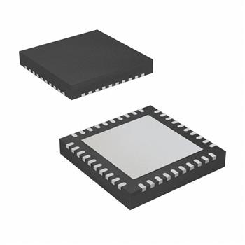
- 封装:40-VFQFN 裸露焊盘
- RoHS:无铅 / 符合限制有害物质指令(RoHS)规范要求
- 包装方式:Digi-Reel®
- 参考价格:$7.067-$9.55
更新日期:2024-04-01 00:04:00
产品简介:2.5V 锁相环路 DDR 时钟驱动器
查看详情- 封装:40-VFQFN 裸露焊盘
- RoHS:无铅 / 符合限制有害物质指令(RoHS)规范要求
- 包装方式:Digi-Reel®
- 参考价格:$7.067-$9.55
CDCVF857RHAT 供应商
- 公司
- 型号
- 品牌
- 封装/批号
- 数量
- 地区
- 日期
- 说明
- 询价
-
TI
-
原厂原装
22+ -
3288
-
上海市
-
-
-
一级代理原装
-
TI ?
-
SMD
5 -
100
-
杭州
-
-
-
原装正品现货
CDCVF857RHAT 中文资料属性参数
- 标准包装:1
- 类别:集成电路 (IC)
- 家庭:时钟/计时 - 时钟发生器,PLL,频率合成器
- 系列:-
- 类型:PLL 时钟驱动器
- PLL:带旁路
- 输入:SSTL-2
- 输出:SSTL-2
- 电路数:1
- 比率 - 输入:输出:2:11
- 差分 - 输入:输出:是/是
- 频率 - 最大:220MHz
- 除法器/乘法器:无/无
- 电源电压:2.3 V ~ 2.7 V
- 工作温度:-40°C ~ 85°C
- 安装类型:表面贴装
- 封装/外壳:40-VFQFN 裸露焊盘
- 供应商设备封装:40-VQFN-EP(6x6)
- 包装:®
- 其它名称:296-18288-6
产品特性
- Spread-Spectrum Clock Compatible
- Operating Frequency: 60 MHz to 220 MHz
- Low Jitter (Cycle-Cycle): ±35 ps
- Low Static Phase Offset: ±50 ps
- Low Jitter (Period): ±30 ps
- 1-to-10 Differential Clock Distribution (SSTL2)
- Best in Class for VOX = VDD/2 ±0.1 V
- Operates From Dual 2.6-V or 2.5-V Supplies
- Available in a 40-Pin MLF Package, 48-Pin TSSOP Package, 56-Ball MicroStar Junior™ BGA Package
- Consumes < 100-µA Quiescent Current
- External Feedback Pins (FBIN, FBIN) Are Used to Synchronize the Outputs to the Input Clocks
- Meets/Exceeds JEDEC Standard (JESD82-1) For DDRI-200/266/333 Specification
- Meets/Exceeds Proposed DDRI-400 Specification (JESD82-1A)
- Enters Low-Power Mode When No CLK Input Signal Is Applied or PWRDWN Is Low
- APPLICATIONSDDR Memory Modules (DDR400/333/266/200)Zero-Delay Fan-Out Buffer
- DDR Memory Modules (DDR400/333/266/200)
- Zero-Delay Fan-Out Buffer
产品概述
The CDCVF857 is a high-performance, low-skew, low-jitter, zero-delay buffer that distributes a differential clock input pair (CLK, CLK) to 10 differential pairs of clock outputs (Y[0:9], Y[0:9]) and one differential pair of feedback clock outputs (FBOUT, FBOUT). The clock outputs are controlled by the clock inputs (CLK, CLK), the feedback clocks (FBIN, FBIN), and the analog power input (AVDD). When PWRDWN is high, the outputs switch in phase and frequency with CLK. When PWRDWN is low, all outputs are disabled to a high-impedance state (3-state) and the PLL is shut down (low-power mode). The device also enters this low-power mode when the input frequency falls below a suggested detection frequency that is below 20 MHz (typical 10 MHz). An input frequency detection circuit detects the low frequency condition and, after applying a >20-MHz input signal, this detection circuit turns the PLL on and enables the outputs.When AVDD is strapped low, the PLL is turned off and bypassed for test purposes. The CDCVF857 is also able to track spread spectrum clocking for reduced EMI.Because the CDCVF857 is based on PLL circuitry, it requires a stabilization time to achieve phase-lock of the PLL. This stabilization time is required following power up. The CDCVF857 is characterized for both commercial and industrial temperature ranges.
CDCVF857RHAT 数据手册
| 数据手册 | 说明 | 数量 | 操作 |
|---|---|---|---|
 CDCVF857RHAT CDCVF857RHAT
|
2.5-V PHASE-LOCK LOOP CLOCK DRIVER |
19 Pages页,476K | 查看 |
|
CDCVF857RHATG4
|
2.5-V PHASE-LOCK LOOP CLOCK DRIVER |
19 Pages页,476K | 查看 |
CDCVF857RHAT 相关产品
- 74HCT4046AD,118
- AD809BRZ-REEL7
- AD9512BCPZ-REEL7
- AD9513BCPZ
- AD9513BCPZ-REEL7
- AD9516-2BCPZ
- AD9516-3BCPZ-REEL7
- AD9517-0ABCPZ-RL7
- AD9517-1ABCPZ
- AD9517-1ABCPZ-RL7
- AD9517-2ABCPZ-RL7
- AD9517-3ABCPZ
- AD9517-3ABCPZ-RL7
- AD9517-4ABCPZ
- AD9517-4ABCPZ-RL7
- AD9518-0ABCPZ
- AD9518-0ABCPZ-RL7
- AD9518-1ABCPZ
- AD9518-1ABCPZ-RL7
- AD9518-2ABCPZ
- AD9518-2ABCPZ-RL7
- AD9518-3ABCPZ-RL7
- AD9518-4ABCPZ
- AD9518-4ABCPZ-RL7
- AD9520-0BCPZ
- AD9522-1BCPZ
- AD9522-2BCPZ
- AD9522-4BCPZ
- AD9522-4BCPZ-REEL7
- AD9522-5BCPZ