 搜索
搜索
 发布采购
发布采购
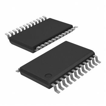
- 封装:24-TSSOP(0.173",4.40mm 宽)
- RoHS:无铅 / 符合限制有害物质指令(RoHS)规范要求
- 包装方式:Digi-Reel®
- 参考价格:$3.1392-$6.28
更新日期:2024-04-01 00:04:00
产品简介:适用于 DRAM 应用且具有 10 个输出的 3.3V 锁相环路时钟驱动器
查看详情- 封装:24-TSSOP(0.173",4.40mm 宽)
- RoHS:无铅 / 符合限制有害物质指令(RoHS)规范要求
- 包装方式:Digi-Reel®
- 参考价格:$3.1392-$6.28
CDCVF2510PWR 供应商
- 公司
- 型号
- 品牌
- 封装/批号
- 数量
- 地区
- 日期
- 说明
- 询价
-
TI
-
原厂原装
22+ -
3288
-
上海市
-
-
-
一级代理原装
-
TI
-
-
2019+ -
5800
-
上海市
-
-
-
全新原装现货
-
TI
-
TSSOP
23+ -
46000
-
合肥
-
-
-
科大讯飞战略投资企业,提供一站式配套服务
CDCVF2510PWR 中文资料属性参数
- 标准包装:1
- 类别:集成电路 (IC)
- 家庭:时钟/计时 - 时钟发生器,PLL,频率合成器
- 系列:-
- 类型:PLL 时钟驱动器
- PLL:带旁路
- 输入:LVTTL
- 输出:LVTTL
- 电路数:1
- 比率 - 输入:输出:2:11
- 差分 - 输入:输出:无/无
- 频率 - 最大:175MHz
- 除法器/乘法器:无/无
- 电源电压:3 V ~ 3.6 V
- 工作温度:0°C ~ 85°C
- 安装类型:表面贴装
- 封装/外壳:24-TSSOP(0.173",4.40mm 宽)
- 供应商设备封装:24-TSSOP
- 包装:®
- 其它名称:296-6725-6
产品特性
- Designed to Meet and Exceed PC133 SDRAM Registered DIMM Specification Rev. 1.1
- Spread Spectrum Clock Compatible
- Operating Frequency 50 MHz to 175 MHz
- Static Phase Error Distribution at 66 MHz to 166 MHz Is ±125 ps
- Jitter (cyc - cyc) at 66 MHz to 166 MHz Is |70| ps
- Advanced Deep Submicron Process Results in More Than 40% Lower Power Consumption Versus Current Generation PC133 Devices
- Available in Plastic 24-Pin TSSOP
- Phase-Lock Loop Clock Distribution for Synchronous DRAM Applications
- Distributes One Clock Input to One Bank of 10 Outputs
- External Feedback (FBIN) Terminal Is Used to Synchronize the Outputs to the Clock Input
- 25- On-Chip Series Damping Resistors
- No External RC Network Required
- Operates at 3.3 V
产品概述
The CDCVF2510 is a high-performance, low-skew, low-jitter, phase-lock loop (PLL) clock driver. It uses a phase-lock loop (PLL) to precisely align, in both frequency and phase, the feedback (FBOUT) output to the clock (CLK) input signal. It is specifically designed for use with synchronous DRAMs. The CDCVF2510 operates at a 3.3-V VCC. It also provides integrated series-damping resistors that make it ideal for driving point-to-point loads.One bank of 10 outputs provides 10 low-skew, low-jitter copies of CLK. Output signal duty cycles are adjusted to 50%, independent of the duty cycle at CLK. Outputs are enabled or disabled via the control (G) input. When the G input is high, the outputs switch in phase and frequency with CLK; when the G input is low, the outputs are disabled to the logic-low state.Unlike many products containing PLLs, the CDCVF2510 does not require external RC networks. The loop filter for the PLL is included on-chip, minimizing component count, board space, and cost.Because it is based on PLL circuitry, the CDCVF2510 requires a stabilization time to achieve phase lock of the feedback signal to the reference signal. This stabilization time is required following power up and application of a fixed-frequency, a fixed-phase signal at CLK, or following any changes to the PLL reference or feedback signals. The PLL can be bypassed for test purposes by strapping AVCC to ground.The CDCVF2510 is characterized for operation from 0°C to 85°C.For application information see the application reports High Speed Distribution Design Techniques for CDC509/516/2509/2510/2516 (SLMA003) and Using CDC2509A/2510A PLL With Spread Spectrum Clocking (SSC) (SCAA039).
CDCVF2510PWR 相关产品
- 74HCT4046AD,118
- AD809BRZ-REEL7
- AD9512BCPZ-REEL7
- AD9513BCPZ
- AD9513BCPZ-REEL7
- AD9516-2BCPZ
- AD9516-3BCPZ-REEL7
- AD9517-0ABCPZ-RL7
- AD9517-1ABCPZ
- AD9517-1ABCPZ-RL7
- AD9517-2ABCPZ-RL7
- AD9517-3ABCPZ
- AD9517-3ABCPZ-RL7
- AD9517-4ABCPZ
- AD9517-4ABCPZ-RL7
- AD9518-0ABCPZ
- AD9518-0ABCPZ-RL7
- AD9518-1ABCPZ
- AD9518-1ABCPZ-RL7
- AD9518-2ABCPZ
- AD9518-2ABCPZ-RL7
- AD9518-3ABCPZ-RL7
- AD9518-4ABCPZ
- AD9518-4ABCPZ-RL7
- AD9520-0BCPZ
- AD9522-1BCPZ
- AD9522-2BCPZ
- AD9522-4BCPZ
- AD9522-4BCPZ-REEL7
- AD9522-5BCPZ