 搜索
搜索
 发布采购
发布采购
- 封装:32-VFQFN 裸露焊盘
- RoHS:无铅 / 符合限制有害物质指令(RoHS)规范要求
- 包装方式:带卷 (TR)
- 参考价格:$4.615
更新日期:2024-04-01 00:04:00

产品简介:1:4 超低抖动晶振时钟发生器
查看详情- 封装:32-VFQFN 裸露焊盘
- RoHS:无铅 / 符合限制有害物质指令(RoHS)规范要求
- 包装方式:带卷 (TR)
- 参考价格:$4.615
CDCM61004RHBR 供应商
- 公司
- 型号
- 品牌
- 封装/批号
- 数量
- 地区
- 日期
- 说明
- 询价
-
TI
-
原厂原装
22+ -
3288
-
上海市
-
-
-
一级代理原装
-
TI/德州仪器
-
VQFN32
21+ -
10000
-
杭州
-
-
-
只做原装现货,大量现货热卖
-
TI(德州仪器)
-
VQFN-32(5x5)
2022+ -
12000
-
上海市
-
-
-
原装可开发票
-
TI
-
VQFN32
21+ -
2500
-
上海市
-
-
-
原装现货!品质为先!请来电垂询!
-
TI
-
VQFN32
22+ -
300000
-
常州
-
-
-
原装正品
-
TI
-
TSSOP
23+ -
46000
-
合肥
-
-
-
科大讯飞战略投资企业,提供一站式配套服务
CDCM61004RHBR 中文资料属性参数
- 标准包装:3,000
- 类别:集成电路 (IC)
- 家庭:时钟/计时 - 时钟发生器,PLL,频率合成器
- 系列:-
- 类型:时钟发生器
- PLL:带旁路
- 输入:LVCMOS,晶体
- 输出:LVCMOS,LVDS,LVPECL
- 电路数:1
- 比率 - 输入:输出:1:5
- 差分 - 输入:输出:无/是
- 频率 - 最大:683.27MHz
- 除法器/乘法器:是/无
- 电源电压:3 V ~ 3.6 V
- 工作温度:-40°C ~ 85°C
- 安装类型:表面贴装
- 封装/外壳:32-VFQFN 裸露焊盘
- 供应商设备封装:32-QFN 裸露焊盘(5x5)
- 包装:带卷 (TR)
产品特性
- One Crystal/LVCMOS Reference Input Including 24.8832 MHz, 25 MHz, and 26.5625 MHz
- Input Frequency Range: 21.875 MHz to 28.47 MHz
- On-Chip VCO Operates in Frequency Range of 1.75 GHz to 2.05 GHz
- 4x Output Available: Pin-Selectable Between LVPECL, LVDS, or 2-LVCMOS; Operates at 3.3 V
- Pin-Selectable Between LVPECL, LVDS, or 2-LVCMOS; Operates at 3.3 V
- LVCMOS Bypass Output Available
- Output Frequency Selectable by /1, /2, /3, /4, /6, /8 from a Single Output Divider
- Supports Common LVPECL/LVDS Output Frequencies: 62.5 MHz, 74.25 MHz, 75 MHz, 77.76 MHz, 100 MHz, 106.25 MHz, 125 MHz, 150 MHz, 155.52 MHz, 156.25 MHz, 159.375 MHz, 187.5 MHz, 200 MHz, 212.5 MHz, 250 MHz, 311.04 MHz, 312.5 MHz, 622.08 MHz, 625 MHz
- 62.5 MHz, 74.25 MHz, 75 MHz, 77.76 MHz, 100 MHz, 106.25 MHz, 125 MHz, 150 MHz, 155.52 MHz, 156.25 MHz, 159.375 MHz, 187.5 MHz, 200 MHz, 212.5 MHz, 250 MHz, 311.04 MHz, 312.5 MHz, 622.08 MHz, 625 MHz
- Supports Common LVCMOS Output Frequencies: 62.5 MHz, 74.25 MHz, 75 MHz, 77.76 MHz, 100 MHz, 106.25 MHz, 125 MHz, 150 MHz, 155.52 MHz, 156.25 MHz, 159.375 MHz, 187.5 MHz, 200 MHz, 212.5 MHz, 250 MHz
- 62.5 MHz, 74.25 MHz, 75 MHz, 77.76 MHz, 100 MHz, 106.25 MHz, 125 MHz, 150 MHz, 155.52 MHz, 156.25 MHz, 159.375 MHz, 187.5 MHz, 200 MHz, 212.5 MHz, 250 MHz
- Output Frequency Range: 43.75 MHz to 683.264 MHz
- Internal PLL Loop Bandwidth: 400 kHz
- High-Performance PLL Core: Phase Noise typically at –146 dBc/Hz at 5-MHz Offset for 625-MHz LVPECL Output Random Jitter typically at 0.509 ps, RMS (10 kHz to 20 MHz) for 625-MHz LVPECL Output
- Phase Noise typically at –146 dBc/Hz at 5-MHz Offset for 625-MHz LVPECL Output
- Random Jitter typically at 0.509 ps, RMS (10 kHz to 20 MHz) for 625-MHz LVPECL Output
- Output Duty Cycle Corrected to 50% (± 5%)
- Low Output Skew of 30 ps on LVPECL Outputs
- Divider Programming Using Control Pins: Two Pins for Prescaler/Feedback Divider Three Pins for Output Divider Two Pins for Output Select
- Two Pins for Prescaler/Feedback Divider
- Three Pins for Output Divider
- Two Pins for Output Select
- Chip Enable Control Pin Available
- 3.3-V Core and I/O Power Supply
- Industrial Temperature Range: –40°C to 85°C
- 5-mm × 5-mm, 32-pin, VQFN (RHB) Package
- ESD Protection Exceeds 2 kV (HBM)
产品概述
The CDCM61004 is a highly versatile, low-jitter frequency synthesizer capable of
generating four low-jitter clock outputs, selectable between low-voltage positive emitter coupled
logic (LVPECL), low-voltage differential signaling (LVDS), or low-voltage complementary metal oxide
semiconductor (LVCMOS) outputs, from a low-frequency crystal of LVCMOS input for a variety of
wireline and data communication applications. The CDCM61004 features an onboard PLL that can be
easily configured solely through control pins. The overall output random jitter performance is less
than 1 ps, RMS (from 10 kHz to 20 MHz), making this device a perfect choice for use in demanding
applications such as SONET, Ethernet, Fibre Channel, and SAN. The CDCM61004 is available in a
small, 32-pin, 5-mm × 5-mm VQFN package.The CDCM61004 is a high-performance, low-phase noise, fully-integrated voltage-controlled
oscillator (VCO) clock synthesizer with four universal output buffers that can be configured to be
LVPECL, LVDS, or LVCMOS compatible. Each universal output can also be converted to two LVCMOS
outputs. Additionally, an LVCMOS bypass output clock is available in an output configuration which
can help with crystal loading to achieve an exact desired input frequency. It has one
fully-integrated, low-noise, LC-based VCO that operates in the
1.75 GHz to 2.05 GHz range.The phase-locked loop (PLL) synchronizes the VCO with respect to the input, which can
either be a low-frequency crystal. The output share an output divider sourced from the VCO core.
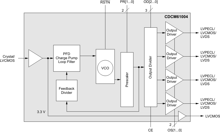
All device settings are managed through a control pin structure, which has two pins that control
the prescaler and feedback divider, three pins that control the output divider, two pins that
control the output type, and one pin that controls the output enable. Any time the PLL settings
(including the input frequency, prescaler divider, or feedback divider) are altered, a reset must
be issued through the Reset control pin (active low for device reset). The reset initiates a PLL
recalibration process to ensure PLL lock. When the device is in reset, the outputs and dividers are
turned off.The output frequency (fOUT) is proportional to the frequency of
the input clock (fIN). The feedback divider, output divider, and VCO
frequency set fOUT with respect to fIN.The output divider can be chosen from 1, 2, 3, 4, 6, or 8 through the use of control
pins. Feedback divider and prescaler divider combinations can be chosen from 25 and 3, 24 and 3, 20
and 4, or 15 and 5, respectively, also through the use of control pins. CDCM61004 Block Diagram shows a high-level diagram of the CDCM61004.The device operates in a 3.3-V supply environment and is characterized for operation from
–40°C to 85°C.
CDCM61004RHBR 电路图
CDCM61004RHBR 电路图
CDCM61004RHBR 相关产品
- 74HCT4046AD,118
- AD809BRZ-REEL7
- AD9512BCPZ-REEL7
- AD9513BCPZ
- AD9513BCPZ-REEL7
- AD9516-2BCPZ
- AD9516-3BCPZ-REEL7
- AD9517-0ABCPZ-RL7
- AD9517-1ABCPZ
- AD9517-1ABCPZ-RL7
- AD9517-2ABCPZ-RL7
- AD9517-3ABCPZ
- AD9517-3ABCPZ-RL7
- AD9517-4ABCPZ
- AD9517-4ABCPZ-RL7
- AD9518-0ABCPZ
- AD9518-0ABCPZ-RL7
- AD9518-1ABCPZ
- AD9518-1ABCPZ-RL7
- AD9518-2ABCPZ
- AD9518-2ABCPZ-RL7
- AD9518-3ABCPZ-RL7
- AD9518-4ABCPZ
- AD9518-4ABCPZ-RL7
- AD9520-0BCPZ
- AD9522-1BCPZ
- AD9522-2BCPZ
- AD9522-4BCPZ
- AD9522-4BCPZ-REEL7
- AD9522-5BCPZ