 搜索
搜索
 发布采购
发布采购
- 封装:48-VFQFN 裸露焊盘
- RoHS:无铅 / 符合限制有害物质指令(RoHS)规范要求
- 包装方式:带卷 (TR)
- 参考价格:$9.6
更新日期:2024-04-01 00:04:00

产品简介:1.8V、11 输出时钟倍频器、分频器、抖动消除器和缓冲器
查看详情- 封装:48-VFQFN 裸露焊盘
- RoHS:无铅 / 符合限制有害物质指令(RoHS)规范要求
- 包装方式:带卷 (TR)
- 参考价格:$9.6
CDCL6010RGZR 供应商
- 公司
- 型号
- 品牌
- 封装/批号
- 数量
- 地区
- 日期
- 说明
- 询价
-
TI
-
原厂原装
22+ -
3288
-
上海市
-
-
-
一级代理原装
-
TI
-
TSSOP
23+ -
46000
-
合肥
-
-
-
科大讯飞战略投资企业,提供一站式配套服务
-
TI/德州仪器
-
QFN48
21+ -
10000
-
杭州
-
-
-
只做原装现货,大量现货热卖
-
TI(德州仪器)
-
VQFN-48(7x7)
2022+ -
12000
-
上海市
-
-
-
原装可开发票
CDCL6010RGZR 中文资料属性参数
- 标准包装:2,500
- 类别:集成电路 (IC)
- 家庭:时钟/计时 - 时钟发生器,PLL,频率合成器
- 系列:-
- 类型:时钟同步器
- PLL:带旁路
- 输入:LVDS
- 输出:CML
- 电路数:1
- 比率 - 输入:输出:1:11
- 差分 - 输入:输出:是/是
- 频率 - 最大:1.25GHz
- 除法器/乘法器:是/是
- 电源电压:1.7 V ~ 1.9 V
- 工作温度:-40°C ~ 85°C
- 安装类型:表面贴装
- 封装/外壳:48-VFQFN 裸露焊盘
- 供应商设备封装:48-VQFN 裸露焊盘(7x7)
- 包装:带卷 (TR)
- 配用:CDCE421EVM-ND - CDCE421EVM
产品特性
- Single 1.8V Supply
- High-Performance Clock Multiplier, Distributor, Jitter Cleaner, and Buffer With 11 Outputs
- Low Output Jitter: 400fs RMS
- Output Group Phase Adjustment
- Low-Voltage Differential Signaling (LVDS) Input, 100Ω Differential On-Chip Termination, 30MHz to 319MHz Frequency Range
- Differential Current Mode Logic (CML) Outputs, 50Ω Single-Ended On-Chip Termination, 15MHz to 1.25GHz Frequency Range
- One Dedicated Differential CML Output, Straight PLL and Frequency Divider Bypass
- Two Groups of Five Outputs Each with Independent Frequency Division Ratios; Optional PLL Bypass
- Fully Integrated Voltage Controlled Oscillator (VCO); Supports Wide Output Frequency Range
- Output Frequency Derived From VCO Frequency with Divide Ratios of 1, 2, 4, 5, 8, 10, 16, 20, 32, 40, and 80
- Meets OBSAI RP1 v1.0 Standard and CPRI v2.0 Requirements
- Meets ANSI TIA/EIA-644-A-2001 LVDS Standard Requirements
- Integrated LC Oscillator Allows External Bandwidth Adjustment
- PLL Lock Indication
- Power Consumption: 640mW Typical
- Output Enable Control for Each Output
- SDA/SCL Device Management Interface
- 48-pin QFN (RGZ) Package
- Industrial Temperature Range: –40°C to +85°C
- APPLICATIONS Low Jitter Clocking for High-Speed SERDES Jitter Cleaning of SERDES Reference Clocks for 1G/10G Ethernet, 1X/2X/4X/10X Fibre Channel, PCI Express, Serial ATA, SONET, CPRI, OBSAI, etc. Up to 1-to-11 Clock Buffering and Fan-out
- Low Jitter Clocking for High-Speed SERDES
- Jitter Cleaning of SERDES Reference Clocks for 1G/10G Ethernet, 1X/2X/4X/10X Fibre Channel, PCI Express, Serial ATA, SONET, CPRI, OBSAI, etc.
- Up to 1-to-11 Clock Buffering and Fan-out
产品概述
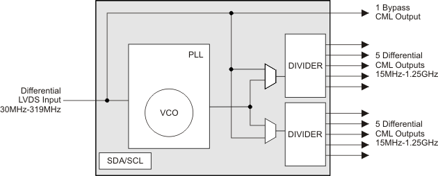
The CDCL6010 is a high-performance, low phase noise clock multiplier, distributor, jitter cleaner, and low skew buffer. It effectively cleans a noisy system clock with a fully-integrated low noise Voltage Controlled Oscillator
(VCO) that operates in the 1.2GHz–1.275GHz range. (Note that the LC oscillator oscillates in the 2.4GHz–2.55GHz range. The frequency is predivided by 2 before the post-dividers P0 and P1.)The output frequency (FOUT) is synchronized to the frequency of the input clock (FIN). The programmable pre-dividers, M and N, and the post-dividers, P0 and P1, give a high flexibility to the ratio of the output frequency to the input frequency:FOUT = FIN × N/(M × P)Where:P (P0, P1) = 1, 2, 4, 5, 8, 10, 16, 20, 32, 40, 80M = 1, 2, 4, 8N = 32, 40provided that:30MHz < (FIN /M) < 40MHz1200MHz < (FOUT × P) < 1275MHzThe PLL loop bandwidth is user-selectable by external filter components or by using the internal loop filter. The PLL loop bandwidth and damping factor can be adjusted to meet different system requirements.The CDCL6010 supports one differential LVDS clock input and a total of 11 differential CML outputs. One output is a straight bypass with no support for jitter cleaning or clock multiplication. The remaining 10 outputs are available in two groups of five outputs each with independent frequency division ratios. Those 10 outputs can be optionally setup to bypass the PLL when no jitter cleaning is needed. The CML outputs are compatible with LVDS receivers if ac-coupled.With careful observation of the input voltage swing and common-mode voltage limits, the CDCL6010 can support a single-ended clock input as outlined in the Pin Description TableThe CDCL6010 can operate as a multi-output clock buffer in a PLL bypass mode.All device settings are programmable through the SDA/SCL, serial two-wire interface.The serial interface is 1.8V tolerant only.The phase of one output group relative to the other can be adjusted through the SDA/SCL interface. For post-divide ratios (P0, P1) that are multiples of 5, the total number of phase adjustment steps (n) equals the divide-ratio divided by 5. For post-divide ratios (P0, P1) that are not multiples of 5, the total number of steps (n) is the same as the post-divide ratio. The phase adjustment step () in time units is given as: = 1/(n × FOUT)where FOUT is the respective output frequency.The device operates in a 1.8V supply environment and is characterized for operation from –40°C to +85°C.The CDCL6010 is available in a 48-pin QFN (RGZ) package.
CDCL6010RGZR 数据手册
| 数据手册 | 说明 | 数量 | 操作 |
|---|---|---|---|
 CDCL6010RGZRG4 CDCL6010RGZRG4
|
1.8V 11-Outputs Clock Multiplier, Distributor, Jitter Cleaner and Buffer 48-QFN -40 to 85 |
25页,569K | 查看 |
CDCL6010RGZR 电路图
CDCL6010RGZR 电路图
CDCL6010RGZR 相关产品
- 74HCT4046AD,118
- AD809BRZ-REEL7
- AD9512BCPZ-REEL7
- AD9513BCPZ
- AD9513BCPZ-REEL7
- AD9516-2BCPZ
- AD9516-3BCPZ-REEL7
- AD9517-0ABCPZ-RL7
- AD9517-1ABCPZ
- AD9517-1ABCPZ-RL7
- AD9517-2ABCPZ-RL7
- AD9517-3ABCPZ
- AD9517-3ABCPZ-RL7
- AD9517-4ABCPZ
- AD9517-4ABCPZ-RL7
- AD9518-0ABCPZ
- AD9518-0ABCPZ-RL7
- AD9518-1ABCPZ
- AD9518-1ABCPZ-RL7
- AD9518-2ABCPZ
- AD9518-2ABCPZ-RL7
- AD9518-3ABCPZ-RL7
- AD9518-4ABCPZ
- AD9518-4ABCPZ-RL7
- AD9520-0BCPZ
- AD9522-1BCPZ
- AD9522-2BCPZ
- AD9522-4BCPZ
- AD9522-4BCPZ-REEL7
- AD9522-5BCPZ