 搜索
搜索
 发布采购
发布采购
- 封装:20-TSSOP(0.173",4.40mm 宽)
- RoHS:无铅 / 符合限制有害物质指令(RoHS)规范要求
- 包装方式:Digi-Reel®
- 参考价格:$3.456-$6.91
更新日期:2024-04-01 00:04:00

产品简介:具有 1.8V LVCMOS 输出的汽车类可编程 3-PLL VCXO 时钟合成器
查看详情- 封装:20-TSSOP(0.173",4.40mm 宽)
- RoHS:无铅 / 符合限制有害物质指令(RoHS)规范要求
- 包装方式:Digi-Reel®
- 参考价格:$3.456-$6.91
CDCEL937QPWRQ1 供应商
- 公司
- 型号
- 品牌
- 封装/批号
- 数量
- 地区
- 日期
- 说明
- 询价
-
TI
-
原厂原装
22+ -
3288
-
上海市
-
-
-
一级代理原装
-
TI/德州仪器
-
21+
TSSOP20 -
10000
-
杭州
-
-
-
只做原装现货,大量现货热卖
-
TSSOP
23+ -
46000
-
合肥
-
-
-
科大讯飞战略投资企业,提供一站式配套服务
CDCEL937QPWRQ1 中文资料属性参数
- 标准包装:1
- 类别:集成电路 (IC)
- 家庭:时钟/计时 - 时钟发生器,PLL,频率合成器
- 系列:-
- 类型:时钟/频率合成器
- PLL:带旁路
- 输入:LVCMOS,晶体
- 输出:LVCMOS
- 电路数:1
- 比率 - 输入:输出:1:7
- 差分 - 输入:输出:无/无
- 频率 - 最大:230MHz
- 除法器/乘法器:是/无
- 电源电压:1.7 V ~ 1.9 V
- 工作温度:-40°C ~ 125°C
- 安装类型:表面贴装
- 封装/外壳:20-TSSOP(0.173",4.40mm 宽)
- 供应商设备封装:20-TSSOP
- 包装:®
- 其它名称:296-27403-6
产品特性
- Qualified for Automotive Applications
- AEC-Q100 Qualified With the Following Results: Device Temperature Grade 1: –40°C to 125°C Ambient Operating Temperature Range Device HBM ESD Classification Level 2 Device CDM ESD Classification Level C4B
- Device Temperature Grade 1: –40°C to 125°C Ambient Operating Temperature Range
- Device HBM ESD Classification Level 2
- Device CDM ESD Classification Level C4B
- In-System Programmability and EEPROM Serial Programmable Volatile Register Nonvolatile EEPROM to Store Customer Setting
- Serial Programmable Volatile Register
- Nonvolatile EEPROM to Store Customer Setting
- Flexible Input Clocking Concept External Crystal: 8 MHz to 32 MHz On-Chip VCXO: Pull Range ±150 ppm Single-Ended LVCMOS up to 160 MHz
- External Crystal: 8 MHz to 32 MHz
- On-Chip VCXO: Pull Range ±150 ppm
- Single-Ended LVCMOS up to 160 MHz
- Free Selectable Output Frequency up to 230 MHz
- Low-Noise PLL Core Integrated PLL Loop Filter Components Low Period Jitter (Typical 60 ps)
- Integrated PLL Loop Filter Components
- Low Period Jitter (Typical 60 ps)
- Separate Output Supply Pins CDCE937-Q1: 3.3 V and 2.5 V CDCEL937-Q1: 1.8 V
- CDCE937-Q1: 3.3 V and 2.5 V
- CDCEL937-Q1: 1.8 V
- Flexible Clock Driver Three User-Definable Control Inputs [S0/S1/S2]; for Example: SSC Selection, Frequency Switching, Output Enable or Power Down Generates Highly Accurate Clocks for Video, Audio, USB, IEEE1394, RFID, Bluetooth™, WLAN, Ethernet™, and GPS Generates Common Clock Frequencies Used With TI-DaVinci™, OMAP™, DSPs Programmable SSC Modulation Enables 0-PPM Clock Generation
- Three User-Definable Control Inputs [S0/S1/S2]; for Example: SSC Selection, Frequency Switching, Output Enable or Power Down
- Generates Highly Accurate Clocks for Video, Audio, USB, IEEE1394, RFID, Bluetooth™, WLAN, Ethernet™, and GPS
- Generates Common Clock Frequencies Used With TI-DaVinci™, OMAP™, DSPs
- Programmable SSC Modulation
- Enables 0-PPM Clock Generation
- 1.8-V Device Power Supply
- Wide Temperature Range –40°C to 125°C
- Packaged in TSSOP
- Development and Programming Kit for Easy PLL Design and Programming (TI Pro-Clock™)
- APPLICATIONS Clusters Head Units Navigation Systems Advanced Driver Assistance Systems (ADAS)
- Clusters
- Head Units
- Navigation Systems
- Advanced Driver Assistance Systems (ADAS)
产品概述
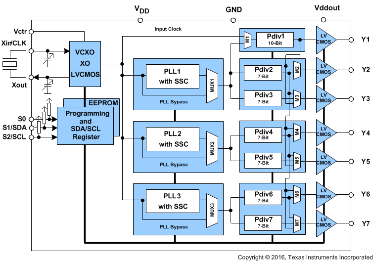
The CDCE937-Q1 and CDCEL937-Q1 devices are modular, phase-locked loop (PLL) based
programmable clock synthesizers. These devices provide flexible and programmable options, such as
output clocks, input signals, and control pins, so that the user can configure the CDCEx937-Q1 for
their own specifications.The CDCEx937-Q1 generates up to seven output clocks from a single input frequency to
enable both board space and cost savings. Additionally, with multiple outputs, the clock generator
can replace multiple crystals with one clock generator. This makes the device well-suited for head
unit and telematics applications in infotainment and camera systems in ADAS as these platforms are
evolving into smaller and more cost effective systems.Furthermore, each output can be programmed in-system for any clock frequency up to 230
MHz through the integrated, configurable PLL. The PLL also supports spread-spectrum clocking (SSC)
with programmable down and center spread. This provides better electromagnetic interference (EMI)
performance to enable customers to pass industry standards such as CISPR-25.Customization of frequency programming and SSC are accessed using three user-defined
control pins. This eliminates the additional interface requirement to control the clock. Specific
power-up and power-down sequences can also be defined to the userΩs needs.
CDCEL937QPWRQ1 电路图
CDCEL937QPWRQ1 电路图
CDCEL937QPWRQ1 相关产品
- 74HCT4046AD,118
- AD809BRZ-REEL7
- AD9512BCPZ-REEL7
- AD9513BCPZ
- AD9513BCPZ-REEL7
- AD9516-2BCPZ
- AD9516-3BCPZ-REEL7
- AD9517-0ABCPZ-RL7
- AD9517-1ABCPZ
- AD9517-1ABCPZ-RL7
- AD9517-2ABCPZ-RL7
- AD9517-3ABCPZ
- AD9517-3ABCPZ-RL7
- AD9517-4ABCPZ
- AD9517-4ABCPZ-RL7
- AD9518-0ABCPZ
- AD9518-0ABCPZ-RL7
- AD9518-1ABCPZ
- AD9518-1ABCPZ-RL7
- AD9518-2ABCPZ
- AD9518-2ABCPZ-RL7
- AD9518-3ABCPZ-RL7
- AD9518-4ABCPZ
- AD9518-4ABCPZ-RL7
- AD9520-0BCPZ
- AD9522-1BCPZ
- AD9522-2BCPZ
- AD9522-4BCPZ
- AD9522-4BCPZ-REEL7
- AD9522-5BCPZ