 搜索
搜索
 发布采购
发布采购
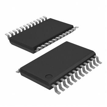
- 封装:24-TSSOP(0.173",4.40mm 宽)
- RoHS:无铅 / 符合限制有害物质指令(RoHS)规范要求
- 包装方式:Digi-Reel®
- 参考价格:$3.6835-$6.84
更新日期:2024-04-01 00:04:00
产品简介:具有 2.5V 或 3.3V LVCMOS 输出的 AEC-Q100 可编程 4-PLL VCXO 时钟合成器
查看详情- 封装:24-TSSOP(0.173",4.40mm 宽)
- RoHS:无铅 / 符合限制有害物质指令(RoHS)规范要求
- 包装方式:Digi-Reel®
- 参考价格:$3.6835-$6.84
CDCE949QPWRQ1 供应商
- 公司
- 型号
- 品牌
- 封装/批号
- 数量
- 地区
- 日期
- 说明
- 询价
-
TI
-
原厂原装
22+ -
3288
-
上海市
-
-
-
一级代理原装
-
TI
-
SMD
2018+ -
4000
-
上海市
-
-
-
原装进口
-
Texas Instruments
-
原厂原装
22+授权代理 -
15800
-
上海市
-
-
-
旋尔只做进口原装,假一赔十...
-
TI(德州仪器)
-
TSSOP-24
2022+ -
9
-
上海市
-
-
-
原装可开发票
CDCE949QPWRQ1 中文资料属性参数
- 标准包装:1
- 类别:集成电路 (IC)
- 家庭:时钟/计时 - 时钟发生器,PLL,频率合成器
- 系列:-
- 类型:时钟合成器
- PLL:带旁路
- 输入:LVCMOS,晶体
- 输出:LVCMOS
- 电路数:1
- 比率 - 输入:输出:1:9
- 差分 - 输入:输出:无/无
- 频率 - 最大:230MHz
- 除法器/乘法器:是/无
- 电源电压:1.7 V ~ 1.9 V
- 工作温度:-40°C ~ 125°C
- 安装类型:表面贴装
- 封装/外壳:24-TSSOP(0.173",4.40mm 宽)
- 供应商设备封装:24-TSSOP
- 包装:®
- 其它名称:296-27402-6
产品特性
- Qualified for Automotive Applications
- Member of Programmable Clock Generator Family CDCE913/CDCEL913: 1 PLLs, 3 Outputs CDCE925/CDCEL925: 2 PLLs, 5 Outputs CDCE937/CDCEL937: 3 PLLs, 7 Outputs CDCE949: 4 PLLs, 9 Outputs
- CDCE913/CDCEL913: 1 PLLs, 3 Outputs
- CDCE925/CDCEL925: 2 PLLs, 5 Outputs
- CDCE937/CDCEL937: 3 PLLs, 7 Outputs
- CDCE949: 4 PLLs, 9 Outputs
- In-System Programmability and EEPROM Serial Programmable Volatile Register Non-Volatile EEPROM to Store Customer Settings
- Serial Programmable Volatile Register
- Non-Volatile EEPROM to Store Customer Settings
- Highly Flexible Clock Driver Three User-Definable Control Inputs [S0/S1/S2]; e.g,. SSC-Selection, Frequency Switching, Output Enable or Power Down Generates Highly-Accurate Clocks for Video, Audio, USB, IEEE1394, RFID, Generates Common Clock Frequencies Used with TI DaVinci™, OMAP™, DSPs BlueTooth™, WLAN, Ethernet and GPS Programmable SSC Modulation Enables 0-PPM Clock Generation
- Three User-Definable Control Inputs [S0/S1/S2]; e.g,. SSC-Selection, Frequency Switching, Output Enable or Power Down
- Generates Highly-Accurate Clocks for Video, Audio, USB, IEEE1394, RFID, Generates Common Clock Frequencies Used with TI DaVinci™, OMAP™, DSPs
- BlueTooth™, WLAN, Ethernet and GPS
- Programmable SSC Modulation
- Enables 0-PPM Clock Generation
- Selectable Output Frequency up to 230 MHz
- Flexible Input Clocking Concept External Crystal: 8 to 32 MHz On-Chip VCXO: Pull-Range ±150 ppm Single-Ended LVCMOS up to 160 MHz
- External Crystal: 8 to 32 MHz
- On-Chip VCXO: Pull-Range ±150 ppm
- Single-Ended LVCMOS up to 160 MHz
- Low-Noise PLL Core Integrated PLL Loop Filter Components Very Low Period Jitter (typ 60 ps)
- Integrated PLL Loop Filter Components
- Very Low Period Jitter (typ 60 ps)
- Separate Output Supply Pins 3.3 V and 2.5 V
- 3.3 V and 2.5 V
- 1.8 V Device Power Supply
- Latch-Up Performace Meets 100 mAPer JESD 78, Class I
- Wide Temperature Range –40°C to 125°C
- Packaged in TSSOP
- Development and Programming Kit for Ease PLL Design and Programming (TI-Pro Clock)
- APPLICATIONS D-TV, HD-TV, STB, IP-STB, DVD-Player, DVD-Recorder, Printer General Purpose Frequency Synthesizing
- D-TV, HD-TV, STB, IP-STB, DVD-Player, DVD-Recorder, Printer
- General Purpose Frequency Synthesizing
产品概述
The CDCE949 is a modular PLL-based low-cost high-performance programmable clock synthesizer, multiplier, and divider. It generates up to 9 output clocks from a single input frequency. Each output can be programmed in-system for any clock frequency up to 230 MHz, using up to four independent configurable PLLs.The CDCE949 has separate output supply pins, VDDOUT, of 2.5 V to 3.3 V. The input accepts an external crystal or LVCMOS clock signal. If an external crystal is used, an on-chip load capacitor is adequate for most applications. The value of the load capacitor is programmable from 0 to 20 pF. Additionally, an on-chip VCXO is selectable, allowing synchronization of the output frequency to an external control signal, that is, a PWM signal.The deep M/N divider ratio allows the generation of zero-ppm audio/video, networking (WLAN, BlueTooth™, Ethernet, GPS) or Interface (USB, IEEE1394, Memory Stick) clocks from a reference input frequency, such as 27 MHz.All PLLs support SSC (Spread-Spectrum Clocking). SSC can be Center-Spread or Down-Spread clocking. This is a common technique to reduce electro-magnetic interference (EMI).Based on the PLL frequency and the divider settings, the internal loop-filter components are automatically adjusted to achieve high stability, and to optimize the jitter-transfer characteristics of each PLL.The device supports non-volatile EEPROM programming for easy customization of the device to the application. It is preset to a factory-default configuration (see the Default device Configuration section). It can be reprogrammed to a different application configuration before PCB assembly, or reprogrammed by in-system programming. All device settings are programmable through the SDA/SCL bus, a 2-wire serial interface.Three programmable control inputs, S0, S1 and S2, can be used to control various aspects of operation including frequency selection, changing the SSC parameters to lower EMI, PLL bypass, power down, and choosing between low level or 3-state for the output-disable function.The CDCE949 operates in a 1.8 V environment. It operates within a temprateure range of –40°C to 125°C.
CDCE949QPWRQ1 相关产品
- 74HCT4046AD,118
- AD809BRZ-REEL7
- AD9512BCPZ-REEL7
- AD9513BCPZ
- AD9513BCPZ-REEL7
- AD9516-2BCPZ
- AD9516-3BCPZ-REEL7
- AD9517-0ABCPZ-RL7
- AD9517-1ABCPZ
- AD9517-1ABCPZ-RL7
- AD9517-2ABCPZ-RL7
- AD9517-3ABCPZ
- AD9517-3ABCPZ-RL7
- AD9517-4ABCPZ
- AD9517-4ABCPZ-RL7
- AD9518-0ABCPZ
- AD9518-0ABCPZ-RL7
- AD9518-1ABCPZ
- AD9518-1ABCPZ-RL7
- AD9518-2ABCPZ
- AD9518-2ABCPZ-RL7
- AD9518-3ABCPZ-RL7
- AD9518-4ABCPZ
- AD9518-4ABCPZ-RL7
- AD9520-0BCPZ
- AD9522-1BCPZ
- AD9522-2BCPZ
- AD9522-4BCPZ
- AD9522-4BCPZ-REEL7
- AD9522-5BCPZ