 搜索
搜索
 发布采购
发布采购
- 封装:48-VFQFN 裸露焊盘
- RoHS:无铅 / 符合限制有害物质指令(RoHS)规范要求
- 包装方式:带卷 (TR)
- 参考价格:$9.6
更新日期:2024-04-01 00:04:00

产品简介:具有集成双通道 VCO 的 5/10 路输出时钟发生器/抖动消除器
查看详情- 封装:48-VFQFN 裸露焊盘
- RoHS:无铅 / 符合限制有害物质指令(RoHS)规范要求
- 包装方式:带卷 (TR)
- 参考价格:$9.6
CDCE62005RGZR 供应商
- 公司
- 型号
- 品牌
- 封装/批号
- 数量
- 地区
- 日期
- 说明
- 询价
-
TI
-
原厂原装
22+ -
3288
-
上海市
-
-
-
一级代理原装
-
TI/德州仪器
-
VQFN48
21+ -
3000
-
杭州
-
-
-
只做原装现货,大量现货热卖
-
TI
-
VQFN48
21+ -
5000
-
上海市
-
-
-
原装现货,品质为先!请来电垂询!
-
TI
-
48VQFN
23+ -
5800
-
上海市
-
-
-
进口原装现货,杜绝假货。
-
-
23+ -
46000
-
合肥
-
-
-
科大讯飞战略投资企业,提供一站式配套服务
CDCE62005RGZR 中文资料属性参数
- 标准包装:2,500
- 类别:集成电路 (IC)
- 家庭:时钟/计时 - 时钟发生器,PLL,频率合成器
- 系列:-
- 类型:时钟发生器
- PLL:带旁路
- 输入:LVCMOS,LVDS,LVPECL,晶体
- 输出:LVCMOS,LVDS,LVPECL
- 电路数:1
- 比率 - 输入:输出:3:10
- 差分 - 输入:输出:是/是
- 频率 - 最大:1.5GHz
- 除法器/乘法器:是/无
- 电源电压:3 V ~ 3.6 V
- 工作温度:-40°C ~ 85°C
- 安装类型:表面贴装
- 封装/外壳:48-VFQFN 裸露焊盘
- 供应商设备封装:48-VQFN 裸露焊盘(7x7)
- 包装:带卷 (TR)
产品特性
- Superior Performance: Low Noise Clock Generator: 550 fs rms typical (10 kHz to 20 MHz Integration Bandwidth), FC = 100 MHz Low Noise Jitter Cleaner: 2.6 ps rms typical (10 kHz to 20 MHz Integration Bandwidth), FC = 100 MHz
- Low Noise Clock Generator: 550 fs rms typical (10 kHz to 20 MHz Integration Bandwidth), FC = 100 MHz
- Low Noise Jitter Cleaner: 2.6 ps rms typical (10 kHz to 20 MHz Integration Bandwidth), FC = 100 MHz
- Flexible Frequency Planning: 5 Fully Configurable Outputs: LVPECL, LVDS, LVCMOS and Special High Swing Output Modes Unique Dual-VCO Architecture Supports a Wide Tuning Range: 1.750 GHz to 2.356 GHz Output Frequency Ranges from 4.25 MHz to 1.175 GHz in Synthesizer Mode Output Frequency up to 1.5 GHz in Fan-Out Mode Independent Coarse Skew Control on all Outputs
- 5 Fully Configurable Outputs: LVPECL, LVDS, LVCMOS and Special High Swing Output Modes
- Unique Dual-VCO Architecture Supports a Wide Tuning Range: 1.750 GHz to 2.356 GHz
- Output Frequency Ranges from 4.25 MHz to 1.175 GHz in Synthesizer Mode
- Output Frequency up to 1.5 GHz in Fan-Out Mode
- Independent Coarse Skew Control on all Outputs
- High Flexibility: Integrated EEPROM Determines Device Configuration at Power-up Smart Input Multiplexer Automatically Switches Between One of Three Reference Inputs
- Integrated EEPROM Determines Device Configuration at Power-up
- Smart Input Multiplexer Automatically Switches Between One of Three Reference Inputs
- 7-mm × 7-mm 48-Pin VQFN Package (RGZ)
- –40°C to +85°C Temperature Range
产品概述
The CDCE62005 is a high performance clock generator and distributor featuring low output
jitter, a high degree of configurability via a SPI interface, and programmable start up modes
determined by on-chip EEPROM. Specifically tailored for clocking data converters and high-speed
digital signals, the CDCE62005 achieves jitter performance well under 1 ps RMS (10 kHz to 20 MHz
integration bandwidth).The CDCE62005 incorporates a synthesizer block with partially integrated loop filter, a
clock distribution block including programmable output formats, and an input block featuring an
innovative smart multiplexer. The clock distribution block includes five individually programmable
outputs that can be configured to provide different combinations of output formats (LVPECL, LVDS,
LVCMOS). Each output can also be programmed to a unique output frequency (up to 1.5 GHz) and skew
relationship via a programmable delay block (note that frequency range depends on operational mode
and output format selected). If all outputs are configured in single-ended mode (for example,
LVCMOS), the CDCE62005 supports up to ten outputs. Each output can select one of four clock sources
to condition and distribute including any of the three clock inputs or the output of the frequency
synthesizer. The input block includes two universal differential inputs which support frequencies
in the range of 40 kHz to 500 MHz and an auxiliary input that can be configured to connect to an
external crystal via an on chip oscillator block.The smart input multiplexer has two modes of operation, manual and automatic. In manual
mode, the user selects the synthesizer reference via the SPI interface. In automatic mode, the
input multiplexer will automatically select between the highest priority input clock
available.
CDCE62005RGZR 电路图
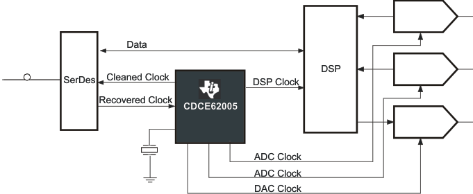
CDCE62005RGZR 电路图
CDCE62005RGZR 相关产品
- 74HCT4046AD,118
- AD809BRZ-REEL7
- AD9512BCPZ-REEL7
- AD9513BCPZ
- AD9513BCPZ-REEL7
- AD9516-2BCPZ
- AD9516-3BCPZ-REEL7
- AD9517-0ABCPZ-RL7
- AD9517-1ABCPZ
- AD9517-1ABCPZ-RL7
- AD9517-2ABCPZ-RL7
- AD9517-3ABCPZ
- AD9517-3ABCPZ-RL7
- AD9517-4ABCPZ
- AD9517-4ABCPZ-RL7
- AD9518-0ABCPZ
- AD9518-0ABCPZ-RL7
- AD9518-1ABCPZ
- AD9518-1ABCPZ-RL7
- AD9518-2ABCPZ
- AD9518-2ABCPZ-RL7
- AD9518-3ABCPZ-RL7
- AD9518-4ABCPZ
- AD9518-4ABCPZ-RL7
- AD9520-0BCPZ
- AD9522-1BCPZ
- AD9522-2BCPZ
- AD9522-4BCPZ
- AD9522-4BCPZ-REEL7
- AD9522-5BCPZ