 搜索
搜索
 发布采购
发布采购
- 封装:32-VFQFN 裸露焊盘
- RoHS:无铅 / 符合限制有害物质指令(RoHS)规范要求
- 包装方式:Digi-Reel®
- 参考价格:$13.3-$17.25
更新日期:2024-04-01 00:04:00

产品简介:具有集成双通道 VCO 的 4 路输出时钟发生器/抖动消除器
查看详情- 封装:32-VFQFN 裸露焊盘
- RoHS:无铅 / 符合限制有害物质指令(RoHS)规范要求
- 包装方式:Digi-Reel®
- 参考价格:$13.3-$17.25
CDCE62002RHBT 供应商
- 公司
- 型号
- 品牌
- 封装/批号
- 数量
- 地区
- 日期
- 说明
- 询价
-
TI
-
原厂原装
22+ -
3288
-
上海市
-
-
-
一级代理原装
-
TI(德州仪器)
-
VQFN-32(5x5)
2022+ -
12000
-
上海市
-
-
-
原装可开发票
-
TI
-
-
23+ -
15000
-
上海市
-
-
-
中国区代理原装进口特价
-
TI
-
时钟合成器
21+ -
6000
-
上海市
-
-
-
原装现货,品质为先!请来电垂询!
-
TI
-
原厂原封装
新批号 -
887000
-
上海市
-
-
-
原厂发货进口原装微信同步QQ893727827
-
TI
-
TSSOP
23+ -
46000
-
合肥
-
-
-
科大讯飞战略投资企业,提供一站式配套服务
CDCE62002RHBT 中文资料属性参数
- 标准包装:1
- 类别:集成电路 (IC)
- 家庭:时钟/计时 - 时钟发生器,PLL,频率合成器
- 系列:-
- 类型:时钟发生器
- PLL:是
- 输入:LVCMOS,LVDS,LVPECL,晶体
- 输出:LVCMOS,LVDS,LVPECL
- 电路数:1
- 比率 - 输入:输出:2:2
- 差分 - 输入:输出:是/是
- 频率 - 最大:1.175GHz
- 除法器/乘法器:是/无
- 电源电压:3 V ~ 3.6 V
- 工作温度:-40°C ~ 85°C
- 安装类型:表面贴装
- 封装/外壳:32-VFQFN 裸露焊盘
- 供应商设备封装:32-QFN 裸露焊盘(5x5)
- 包装:®
- 其它名称:296-24660-6
产品特性
- Frequency Synthesizer With PLL/VCO and Partially Integrated Loop Filter
- Fully Configurable Outputs Including Frequency and Output Format
- Smart Input Multiplexer Automatically Switches Between One of Two Reference Inputs
- Multiple Operational Modes Include Clock Generation Through Crystal, SERDES Start-Up Mode, Jitter Cleaning, and Oscillator Based Holdover Mode
- Integrated EEPROM Determines Device Configuration at Power Up
- Excellent Jitter Performance
- Integrated Frequency Synthesizer Including PLL, Multiple VCOs, and Loop Filter: Full Programmability Facilitates Phase Noise Performance Optimization Enabling Jitter Cleaner Mode Programmable Charge Pump Gain and Loop Filter Settings Unique Dual-VCO Architecture Supports a Wide Tuning Range 1.750 GHz to 2.356 GHz.
- Full Programmability Facilitates Phase Noise Performance Optimization Enabling Jitter Cleaner Mode
- Programmable Charge Pump Gain and Loop Filter Settings
- Unique Dual-VCO Architecture Supports a Wide Tuning Range 1.750 GHz to 2.356 GHz.
- Universal Output Blocks Support Up to 2 Differential, 4 Single-Ended, or Combinations of Differential or Single-Ended: 0.5 ps RMS (10 kHz to 20 MHz) Output Jitter Performance Low Output Phase Noise: –130 dBc/Hz at 1 MHz Offset, Fc = 491.52 MHz Output Frequency Ranges From 10.94 MHz to 1.175 GHz in Synthesizer Mode LVPECL, LVDS, and LVCMOS Independent Output Dividers Support Divide Ratios for 1, 2, 3, 4, 5, 8, 10, 12, 16, 20, 24, and 32
- 0.5 ps RMS (10 kHz to 20 MHz) Output Jitter Performance
- Low Output Phase Noise: –130 dBc/Hz at 1 MHz Offset, Fc = 491.52 MHz
- Output Frequency Ranges From 10.94 MHz to 1.175 GHz in Synthesizer Mode
- LVPECL, LVDS, and LVCMOS
- Independent Output Dividers Support Divide Ratios for 1, 2, 3, 4, 5, 8, 10, 12, 16, 20, 24, and 32
- Flexible Inputs With Innovative Smart Multiplexer: Two Universal Differential Inputs Accept Frequencies from 1 MHz up to 500 MHz (LVPECL), 500 MHz (LVDS), or 250 MHz (LVCMOS) One Auxiliary Input Accepts Crystals in the Range of 2 MHz to 42 MHz Clock Generator Mode Using Crystal Input Smart Input Multiplexer Can be Configured to Automatically Switch Between Highest Priority Clock Source Available Allowing for Fail-Safe Operation
- Two Universal Differential Inputs Accept Frequencies from 1 MHz up to 500 MHz (LVPECL), 500 MHz (LVDS), or 250 MHz (LVCMOS)
- One Auxiliary Input Accepts Crystals in the Range of 2 MHz to 42 MHz
- Clock Generator Mode Using Crystal Input
- Smart Input Multiplexer Can be Configured to Automatically Switch Between Highest Priority Clock Source Available Allowing for Fail-Safe Operation
- Typical Power Consumption 750 mW at 3.3 V
- Integrated EEPROM Stores Default Settings; Therefore, the Device Can Power Up in a Known, Predefined State
- Offered in QFN-32 Package
- ESD Protection Exceeds 2000 V HBM
- Industrial Temperature Range: –40°C to +85°C
- APPLICATIONS Data Converter and Data Aggregation Clocking Wireless Infrastructure Switches and Routers Medical Electronics Military and Aerospace Industrial Clock Generation and Jitter Cleaning
- Data Converter and Data Aggregation Clocking
- Wireless Infrastructure
- Switches and Routers
- Medical Electronics
- Military and Aerospace
- Industrial
- Clock Generation and Jitter Cleaning
产品概述
The CDCE62002 device is a high-performance clock generator featuring low output jitter, a
high degree of configurability through a SPI interface, and programmable start-up modes determined
by on-chip EEPROM. Specifically tailored for clocking data converters and high-speed digital
signals, the CDCE62002 achieves jitter performance under 0.5 ps RMS(1).It incorporates a synthesizer block with partially integrated loop filter, a clock
distribution block including programmable output formats, and an input block featuring an
innovative smart multiplexer. The clock distribution block includes two individually programmable
outputs that can be configured to provide different combinations of output formats (LVPECL, LVDS,
LVCMOS). Each output can also be programmed to a unique output frequency (ranging from 10.94 MHz to
1.175 GHz(2)). If Both outputs are configured in single-ended mode (such as LVCMOS), the CDCE62002 supports up to four outputs. The input block includes one universal differential inputs which support frequencies up to 500 MHz and an auxiliary input that can be configured to connect to an external AT-Cut crystal through an onboard oscillator block. The smart
input multiplexer has two modes of operation, manual and automatic. In manual mode, the user
selects the synthesizer reference through the SPI interface. In automatic mode, the input
multiplexer will automatically select between the highest priority input clock available.(1) 10-kHz to 20-MHz integration bandwidth.
(2) Frequency range depends on operational mode and output format selected.
CDCE62002RHBT 电路图
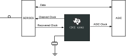
CDCE62002RHBT 电路图
CDCE62002RHBT 相关产品
- 74HCT4046AD,118
- AD809BRZ-REEL7
- AD9512BCPZ-REEL7
- AD9513BCPZ
- AD9513BCPZ-REEL7
- AD9516-2BCPZ
- AD9516-3BCPZ-REEL7
- AD9517-0ABCPZ-RL7
- AD9517-1ABCPZ
- AD9517-1ABCPZ-RL7
- AD9517-2ABCPZ-RL7
- AD9517-3ABCPZ
- AD9517-3ABCPZ-RL7
- AD9517-4ABCPZ
- AD9517-4ABCPZ-RL7
- AD9518-0ABCPZ
- AD9518-0ABCPZ-RL7
- AD9518-1ABCPZ
- AD9518-1ABCPZ-RL7
- AD9518-2ABCPZ
- AD9518-2ABCPZ-RL7
- AD9518-3ABCPZ-RL7
- AD9518-4ABCPZ
- AD9518-4ABCPZ-RL7
- AD9520-0BCPZ
- AD9522-1BCPZ
- AD9522-2BCPZ
- AD9522-4BCPZ
- AD9522-4BCPZ-REEL7
- AD9522-5BCPZ