 搜索
搜索
 发布采购
发布采购
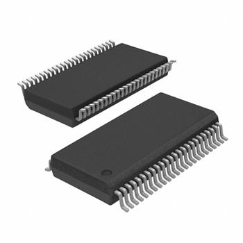
- 封装:48-TFSOP(0.240",6.10mm 宽)
- RoHS:无铅 / 符合限制有害物质指令(RoHS)规范要求
- 包装方式:管件
- 参考价格:$11-$9.9
更新日期:2024-04-01 00:04:00
产品简介:具有三态输出的 3.3V 相位锁定环路时钟驱动器
查看详情- 封装:48-TFSOP(0.240",6.10mm 宽)
- RoHS:无铅 / 符合限制有害物质指令(RoHS)规范要求
- 包装方式:管件
- 参考价格:$11-$9.9
CDC516DGG 供应商
- 公司
- 型号
- 品牌
- 封装/批号
- 数量
- 地区
- 日期
- 说明
- 询价
-
TI
-
原厂原装
22+ -
3288
-
上海市
-
-
-
一级代理原装
-
TI(德州仪器)
-
TSSOP-48
2022+ -
12000
-
上海市
-
-
-
原装可开发票
CDC516DGG 中文资料属性参数
- 标准包装:40
- 类别:集成电路 (IC)
- 家庭:时钟/计时 - 时钟发生器,PLL,频率合成器
- 系列:-
- 类型:PLL 时钟驱动器
- PLL:带旁路
- 输入:LVTTL
- 输出:LVTTL
- 电路数:1
- 比率 - 输入:输出:1:16
- 差分 - 输入:输出:无/无
- 频率 - 最大:125MHz
- 除法器/乘法器:无/无
- 电源电压:3 V ~ 3.6 V
- 工作温度:0°C ~ 70°C
- 安装类型:表面贴装
- 封装/外壳:48-TFSOP(0.240",6.10mm 宽)
- 供应商设备封装:48-TSSOP
- 包装:管件
- 其它名称:296-20833-5
产品特性
- Use CDCVF2510A as a Replacement for this Device
- Phase-Lock Loop Clock Distribution for Synchronous DRAM Applications
- Distributes One Clock Input to Four Banks of Four Outputs
- Separate Output Enable for Each Output Bank
- External Feedback Pin (FBIN) Is Used to Synchronize the Outputs to the Clock Input
- No External RC Network Required
- Operates at 3.3-V VCC
- Packaged in Plastic 48-Pin Thin Shrink Small-Outline Package
产品概述
The CDC516 is a high-performance, low-skew, low-jitter, phase-lock loop clock driver. It uses a phase-lock loop (PLL) to precisely align, in both frequency and phase, the feedback output (FBOUT) to the clock (CLK) input signal. It is specifically designed for use with synchronous DRAMs. The CDC516 operates at 3.3-V VCC and is designed to drive up to five clock loads per output.Four banks of four outputs provide 16 low-skew, low-jitter copies of the input clock. Output signal duty cycles are adjusted to 50 percent, independent of the duty cycle at the input clock. Each bank of outputs can be enabled or disabled separately via the 1G, 2G, 3G, and 4G control inputs. When the G inputs are high, the outputs switch in phase and frequency with CLK; when the G inputs are low, the outputs are disabled to the logic-low state.Unlike many products containing PLLs, the CDC516 does not require external RC networks. The loop filter for the PLL is included on-chip, minimizing component count, board space, and cost.Because it is based on PLL circuitry, the CDC516 requires a stabilization time to achieve phase lock of the feedback signal to the reference signal. This stabilization time is required following power up and application of a fixed-frequency, fixed-phase signal at CLK, as well as following any changes to the PLL reference or feedback signals. The PLL may be bypassed for test purposes by strapping AVCC to ground.The CDC516 is characterized for operation from 0°C to 70°C.
CDC516DGG 数据手册
 CDC516DGG
CDC516DGG 相关产品
- 74HCT4046AD,118
- AD809BRZ-REEL7
- AD9512BCPZ-REEL7
- AD9513BCPZ
- AD9513BCPZ-REEL7
- AD9516-2BCPZ
- AD9516-3BCPZ-REEL7
- AD9517-0ABCPZ-RL7
- AD9517-1ABCPZ
- AD9517-1ABCPZ-RL7
- AD9517-2ABCPZ-RL7
- AD9517-3ABCPZ
- AD9517-3ABCPZ-RL7
- AD9517-4ABCPZ
- AD9517-4ABCPZ-RL7
- AD9518-0ABCPZ
- AD9518-0ABCPZ-RL7
- AD9518-1ABCPZ
- AD9518-1ABCPZ-RL7
- AD9518-2ABCPZ
- AD9518-2ABCPZ-RL7
- AD9518-3ABCPZ-RL7
- AD9518-4ABCPZ
- AD9518-4ABCPZ-RL7
- AD9520-0BCPZ
- AD9522-1BCPZ
- AD9522-2BCPZ
- AD9522-4BCPZ
- AD9522-4BCPZ-REEL7
- AD9522-5BCPZ