 搜索
搜索
 发布采购
发布采购
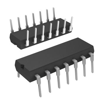
- 封装:14-DIP(0.300",7.62mm)
- RoHS:无铅 / 符合限制有害物质指令(RoHS)规范要求
- 包装方式:管件
- 参考价格:$0.13635-$0.48
更新日期:2024-04-01 00:04:00
产品简介:CMOS 双路 2 宽度双输入与或非门
查看详情- 封装:14-DIP(0.300",7.62mm)
- RoHS:无铅 / 符合限制有害物质指令(RoHS)规范要求
- 包装方式:管件
- 参考价格:$0.13635-$0.48
CD4085BE 供应商
- 公司
- 型号
- 品牌
- 封装/批号
- 数量
- 地区
- 日期
- 说明
- 询价
-
TI
-
原厂原装
22+ -
3288
-
上海市
-
-
-
一级代理原装
-
TI
-
DIP
22+授权代理 -
15800
-
上海市
-
-
-
旋尔只做进口原装,假一赔十...
-
TI(德州仪器)
-
PDIP-14
2022+ -
12000
-
上海市
-
-
-
原装可开发票
CD4085BE 中文资料属性参数
- 标准包装:25
- 类别:集成电路 (IC)
- 家庭:逻辑 - 栅极和逆变器 - 多功能,可配置
- 系列:4000B
- 逻辑类型:与/或/反相门
- 电路数:2
- 输入数:8 输入(2,2,2,2)
- 施密特触发器输入:无
- 输出类型:单端
- 输出电流高,低:6.8mA,6.8mA
- 电源电压:3 V ~ 18 V
- 工作温度:-55°C ~ 125°C
- 安装类型:通孔
- 封装/外壳:14-DIP(0.300",7.62mm)
- 供应商设备封装:14-PDIP
- 包装:管件
- 其它名称:296-3522-5
产品特性
- Medium-speed operation - tPHL = 90 ns; tPLH = 125 ns (typ.) at 10 V
- Individual inhibit controls
- Standardized symmetrical output characteristics
- 100% tested for quiescent current at 20 V
- Maximum input current of 1 µA at 18 V over full package-temperature range; 100 nA at 18 V and 25°C
- Noise margin (over full package-temperature range): 1 V at VDD = 5 V 2 V at VDD = 10 V 2.5 V at VDD = 15 V
- 1 V at VDD = 5 V
- 2 V at VDD = 10 V
- 2.5 V at VDD = 15 V
- 5-V, 10-V, and 15-V parametric ratings
- Meets all requirements of JEDEC Tentative Standard No. 13B, "Standard Specifications for Description of 'B' Series CMOS Devices"
产品概述
CD4085 contains a pair of AND-OR-INVERT gates, each consisting of two 2-input AND gates driving a 3-input NOR gate. Individual inhibit controls are provided for both A-O-I gates.The CD4085B types are supplied in 14-lead hermetic dual-in-line ceramic packages (F3A suffix), 14-lead dual-in-line plastic packages (E suffix), 14-lead small-outline packages (M, MT, M96, and NSR suffixes), and 14-lead thin shrink small-outline packages (PW and PWR suffixes).
 CD4085BE
CD4085BE 相关产品
- 100302QC
- 100307QC
- 74AUP1G97L6X
- 74LVC1G3208DBVRG4
- 74LVC1G57GW,125
- 74LVC1G58GW,125
- CD4019BE
- CD4019BM96
- CD4019BNSR
- CD4019BPWR
- CD4048BE
- CD4048BM96
- CD4048BPW
- CD4068BE
- CD4068BEE4
- CD4068BM96
- CD4068BNSR
- CD4068BPWR
- CD4078BE
- CD4078BM96
- CD4078BNSR
- CD4078BPWR
- CD4078BPWRE4
- CD4085BM
- CD4085BPWR
- CD4086BE
- CD4086BM
- CD4086BMT
- CD4572UBE
- CD4572UBEE4